Single-Stage High Power Factor Flyback for LED Lighting
Abstract
The application note illustrates how the single-stage high power factor flyback converter uses few components and a simple control method to increase input power factor (PF) and reduce input harmonic current. Its content includes the definition of PF, the operating principle of single-stage high power factor flyback converters, peak-current mode control, constant on-time control, feed-forward compensation and total harmonic distortion (THD) optimization.
1. Introduction
In recent years, the technology of light-emitting diodes (LED) has developed rapidly. As it has many advantages, such as high illumination efficiency, long service life, and being mercury free, it has been considered the main illumination source for the next generation. As the increasing environmentally friendly, the expectancy of LED is not only the higher brightness, but also the tougher energy saving requirement. Energy Star stipulates that the power factor of the lighting drivers for housing with power higher than 5W should be higher than 0.7, and that of commercial lighting driver should be higher than 0.9. The application note will discuss how LED lighting drivers use few components and a simple control method to increase input power factor (PF) and reduce input harmonic current in order to meet the requirements of the regulations and save energy.
2. Power Factor
Since our energy is running short, we people pay more attention to put more emphasis on the electrical efficiency of electronic devices. Most conventional power converters use a diode rectifier and electrolytic capacitor to rectify input power source. Although the structure is very simple, it results in serious non-linear distortion and creates a great number of low-frequency harmonics, which brings about a low power factor. Power factor is the ratio of real power and apparent power ;and it is the indicator and to determine its electrical efficiency. If the power factor is low, it will need more current to achieve the desired power output. If the current is increased, the energy loss of the circuit system will increase, too. Therefore, the capacitance of the related electrical equipment will also rise. In order to compensate for the cost of the equipment with capacity large capacitance and energy waste, the power company will charge more electricity fees from its industrial and commercial customers through a higher rates.
The definition of the power factor is as follows :

where P stands for the real power, S stands for the apparent power, which is the product of the root mean square of the input voltage and that of the input current. The real power of a pure resistor load is equal to its apparent power, so its power factor is 1.
If the load is a linear load consisting of inductors, capacitors and resistors, energy may repeatedly flow between the load and the power source, which will result in the reduction of the real power. If the circuit is composed of linear components and the voltage is a sine wave, the current will also be a sine wave with the same frequency; and the relation between the apparent power and real power will be :

where θ is the phase angle between the current and the voltage, and the power factor is cosθ, which is also called the displacement power factor (DPF).
If there are other components different from inductors, capacitors and resistors in the load (non-linear load), the waveform of the input current may distort. Apparent power includes all harmonics. Thus, the power factor will not only be influenced by the displacement power factor resulting from the phase difference between the voltage and the current, but also the distortion power factor corresponding to the harmonics. Its definition is as follows:

where THDi is the total harmonic distortion of the load current. I1,rms is the baseband component of the current, Irms is the total current, and both are expressed by root mean square. The above definition assumes that the voltage is still a sine wave without distortion. The assumption is very close to practical situations. The total power factor can be acquired by multiplying the distortion power factor by the displacement power factor, which is also called the real power factor or power factor :

In order to unify the power factor of electronic devices, European Union regulates the harmonic standard-EN61000-3-2. For the purpose of passing the standard, electronic devices should have the power factor correction (PFC) technology. The application note will introduce the high power factor circuit for LED lighting later.
3. The Operating Principle of the High Power Factor Flyback Converter
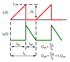
In general, the power of LED lamp is lower than 100W. Thus, it is more appropriate to operate the power converter for driving LED lamp in critical conduction mode (CRM) or discontinuous conduction mode (DCM). Among all kinds of isolated switching converters, the flyback converter has least components and simplest structure. Therefore, LED lighting drivers usually use flyback converters operated in CRM or DCM. The circuit is shown in figure 1, and figure 2 is the ideal current waveform. According to the volt-second balance principle, the relation between the output voltage VO and input voltage Vin is as follows:
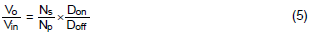
where Don stands for the conduction duty ratio of the power switch Q1, and Doff stands for the conduction duty ratio of output diode DO, as shown in figure 2.
The current-ripple of the magnetizing inductance L of the transformer TX1 can be derived from Faraday’s law, which is as follows :

In CRM or DCM, the current will drop to zero at each switching period. Hence, the current-ripple will be equal to the peak current, as shown in equation (7).

If the input voltage is a sine wave, the input voltage will be as follows :

where ω = 2π • fL ,fL is the input voltage frequency. Assuming that the on-time of the power switch can be controlled constant, and then the following equation can be derived :

That is to say, the peak current of the inductor is a sine wave with the same phase with the voltage, and its peak value is IL,pk.

If there is an electromagnetic interference (EMI) filter in front of the bridge-type rectifier, the angular frequency of the differential mode of the EMI filter will much lower than the switching frequency of the power switch Q1, but higher than the frequency fL of the input voltage. Thus, the input current is just the average value of the inductor ripple. According to the triangle averaging method, the input current can be expressed as the equation (11).

If it is operated in DCM, ts(t) is constant. Therefore, the controller can make input current iin(t) and input voltage Vin(t) have the same phase just by keeping ton(t) unchanged. Accordingly, the power factor is 1 in theory.
If it is operated in CRM, ts(t) will vary with in(t). Therefore, iin(t) and Vin(t) will not have the same phase even if the controller makes ton(t) constant. For this reason, the PF and THD of the flyback converter operated in CRM are slightly lower than that of the flyback converter operated in DCM. However, the peak current will be higher and it is more difficult to eliminate the EMI if it is operated in DCM. Hence, both of the controllers operated in DCM and CRM are useful.
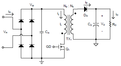
Figure 1. The circuit diagram of the flyback converter
(a) CRM
(b) DCM
Figure 2. The ideal current waveform diagram of the flyback converter
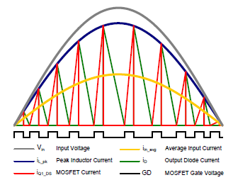
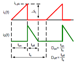
Figure 3. The ideal current waveform diagram of the CRM flyback converter
Figure 3 is the ideal current waveform of the flyback converter operated in CRM. Assuming that the power factor is 1, the root mean square of the input current can be expressed by  the peak value of the average current. Based on the power relation, equation (12) can be derived.
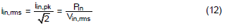
Equation (13), as follows, can be derived from equation (11) :

where ton,pk stands for ton of the input current with the peak value, so is ts,pk.
According to (10), (12) and (13), ton,pk can be expressed as follows :
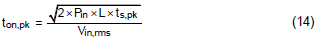
From equation (14), it is obviously that the on-time ton will vary with the input voltage, input power, inductor L and switching period ts.
4. Peak Current Control and Constant On-time Control
Two common PFC control methods are peak current control and constant on-time control. They will be illustrated later.
1.Peak current control :
The input voltage should be detected if peak current PFC control is adopted. The function block diagram of the peak current PFC control is shown in figure. 4. In figure 4, VM is the rectified AC line voltage. VM is divided by resistors RM1, RM2 and then enter the controller. Feedback signal VFB and reference voltage VREF pass through a low-frequency operational transconductance amplifier (OTA) to form the voltage VCOMP, and then VCOMP is multiplied by VMULT. Feedback signal VFB may come from the voltage division of the output voltage, the output current detection or primary side regulation (PSR). If the bandwidth of the OTA is controlled to be much lower than input voltage frequency, the output VCOMP will be a DC voltage with very low ripple. Thus, the output voltage VMO of the multiplier is proportional to VM. In other word, it is proportional to the input voltage. If the voltage CS related to the inductor peak current is equivalent to the output voltage of the multiplier VMO, and the pulse width modulation (PWM) signal is reset to be OFF to turn off the power switch Q1. The inductor peak current will be a sine wave with the same phase with the input voltage, which can achieve high power factor.
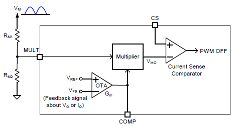
Figure 4. The function block diagram of the peak current PFC control
2.Constant on-time control :
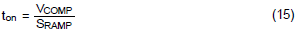
The function block diagram of the constant on-time PFC control is shown in figure 5. It uses a ramp generator rather than a multiplier which is expensive and more complex. The simple ramp generator does not need to detect input voltage, and it will generate a voltage ramp VRAMP with a constant slope SRAMP. When VRAMP is equal to VCOMP, the PWM signal is reset to be OFF to turn off the power switch Q1. The way to generate VCOMP is the same with the peak current PFC control. That is to say, the voltage VCOMP can also be generated by making feedback signal VFB and reference
voltage VREF pass through an OTA. Similarly, if the bandwidth of the OTA is controlled to be much lower than input voltage frequency, the output VCOMP will be a DC voltage with very low ripple. Within one period of the line voltage, if VCOMP is almost constant and the slope SRAMP of VRAMP is also constant, the one-time ton of the power switch Q1 will be constant, as shown in equation (15). Consequently, the inductor peak current will be a sine wave with same phase with the input voltage, which can achieve high power factor.
The appropriate operation range of VCOMP is limited by the linear region of the OTA. It is usually designed to be about 0.8~4.2V. If the slope SRAMP is fixed by the controller, the one-time ton will also be limited. According to equation (14), it is apparent that one-time ton is related to the inductor L under specific input voltages and input powers. Moreover, if the one-time ton is limited, the selection of the inductor will be limited, too. Thus, a RAMP pin may be arranged at some controllers for users to connect external resistors or capacitors to adjust the slope SRAMP so as to expand the application range of the controller.
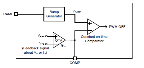
Figure 5. The function block diagram of the constant on-time PFC control
Both of the above two control methods can be operated in CRM or DCM. If in CRM, the controller should have a zero current detection circuit. When detecting that the secondary current of the flyback converter drops to zero, the controller turns on the power switch Q1. If in DCM, the controller should have an oscillator in order to turn on the power switch Q1 at the constant period ts. An RT (or CT) pin may be arranged at some DCM controllers for users to connect external resistors or capacitors to adjust the period ts.
5. Input Voltage Feed-forward Compensation
When the constant on-time PFC control is adopted, no matter whether the controller has the RAMP pin for users to adjust the slope SRAMP or not, the different input voltages will result in different COMP voltage level VCOMP. In the controller, the load level is usually estimated according to VCOMP. For example, if VCOMP is lower than a certain voltage, the controller will operate in the burst mode to increase the efficiency at the light load. If different input voltages are corresponding to different VCOMP, the load level entering the burst mode will be different, too, which is not a proper design. The PFC controllers RT7300 and RT7302 manufactured by Richtek provide the input voltage feed-forward compensation for the constant on-time control, which can keep VCOMP almost unchanged under different input voltages. Figure 6 is the function block diagram of the constant on-time PFC control with the input voltage feed-forward compensation. The input of the OTA is voltage Vset, and its output charge the capacitor CRAMP until the voltage VRAMP is equal to the control voltage VCOMP. The time period is the constant on-time ton.
where the capacitor CRAMP and the transconductance GmRAMP are set by the controller. The VCOMP is acquired by stabilizing the voltage of the negative feedback. Combine equation (14) and equation (16), the VCOMP can be expressed as follows :

According to equation (17), it can be seen that if the Vset is fixed in the controller, VCOMP will be inversely proportional to Vin,rms. In figure 6, VM is the rectified AC line voltage. VM is divided by the resistors RM1 and RM2, and the controller will detect its peak value VMULT,pk and multiply it by the constant k to act as Vset. Thus, Vset can be expressed as follows :

By substituting equation (18) into equation (17) :

Therefore, if the system parameters are constant, VCOMP will only vary with Pin instead of the input voltage. Hence, feed-forward compensation can be achieved.
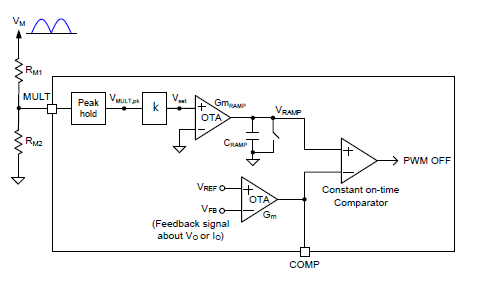
Figure 6. The function block diagram of the constant on-time PFC control with input voltage feed-forward compensation
In the previous chapters, it is mentioned that the PF and THD of the flyback converter operated in CRM are, theoretically, slightly lower than in DCM. The application note provides a kind of THD optimizer, which can effectively improve the PF and THD of the flyback converter operated in CRM.
Substitute equation (9) into equation (11) :

From equation (20), it can be seen that if the on-time ton of the power switch is kept unchanged, the input current iin and input voltage Vin still have the relation of conduction duty ratio Don. If ton can be controlled to be inversely proportional to Don, iin and Vin can almost have the same phase. The switching period of the power switch is much lower than the input voltage period. Hence, there is almost no delay during the whole input voltage period if the Don of previous switching period is used to adjust the ton of the current period. Please refer to figure 7, the THD optimizer is inserted between the Vset and the OTA, and the ramp slope is modulated by the PWM signal. The ideal waveform of the THD optimizer is shown in figure 8.
Accordingly, Vset2 can be expressed as follows :

Substitute equation (21) into equation (16) :

As shown in equation (22), ton is inversely proportional to Don by adopting the THD optimizer, so iin and Vin can almost have the same phase. Figure 9 is the measured waveform of the input voltage Vin and the input current iin, where the input voltage is 230VAC, the output voltage is 30V and the output current is 350mA. Under the same system parameters, the THD of the controller without the THD optimizer is about 13.83%. After THD optimizer is adopted, the THD is reduced to 5.28%. From the measured waveform, it is obviously that the waveform of the input current is closer to the sine wave with the same phase with the input voltage after the THD optimizer is adopted.

Figure 7. THD optimizer
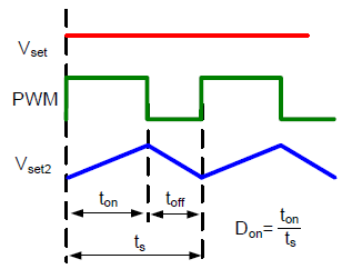
Figure 8. The ideal waveform of the THD optimizer
7. Conclusion
The application note illustrates the operating principle of the single-stage high power factor flyback converter and describes the constant on-time PFC control can work with input voltage feed-forward compensation to keep COMP voltage level almost constant under different input voltages. In addition, the flyback converter with THD optimizer can significantly decrease input current harmonic, which is verified by implementation results.
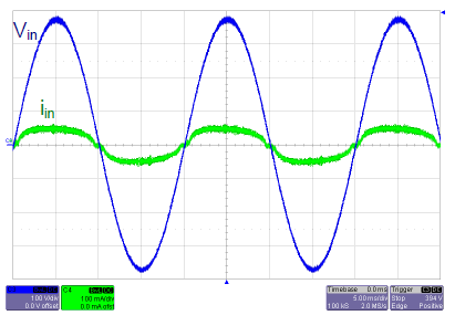
(a) Without THD optimizer
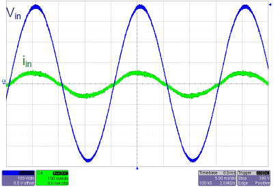
(b) With THD optimizer
(Vin : 100V/div, iin : 100mA/div, time : 5ms/div)
Figure 9. The measured waveforms of the input voltage and the input current