Feedback Control Design of Off-line Flyback Converter
Abstract
Controlling the feedback of off-line flyback converters has often perplexed power engineers because it involves the continuous conduction mode (CCM) and discontinuous conduction mode (DCM) small signal models. Due to the unique feedback compensation mode of the TL431 along with the optocouplers, tuning the feedback parameters still relies on trial and error. This application note provides comprehensive design guidelines, from illustrating power circuit transfer function to designing the circuitry for the TL431 and the optocouplers, to assisting system designers to gain a good phase margin so as to meet the requirements of transient stability. In this note, theoretical computations are done by Mathcad software and verified by Simplis. This method will be applicable to all applications with RT773x series off-line flyback controllers.
1. Scope of Applications: Secondary-Side Flyback Converters
Most flyback converters use secondary-side peak current-mode control of the secondary-side converters to adjust feedback for the output voltages as in Figure 1. The secondary-side output voltage is fed back through the TL431 and the optocoupler to the primary-side. The output of the optocoupler, VCOMP, is compared with the primary-side peak current. This result serves as the negative feedback to the loop and then determines the duty cycle of the switching component Q. RS is the resistor for the primary-stage current detection. CTR is the current transfer ratio of the optocoupler. GFB is the small-signal gain. (Note: It is designed to be about 1/3 of gain internally for all the RT773x ICs.) Se is added externally as the slope compensation to eliminate sub-harmonic oscillation.
Some basic assumptions are made to facilitate the following derivations and explanations as below:
1.Switching component, Q, and the diode in the secondary-side, D, are ideal.
2.The transformer is ideal.
3.The open-loop gain of the TL431 is infinity. (Its nominal open-loop gain is about 50 ~ 60 dB.)
4.The current transfer ratio, CTR, of the optocoupler is a constant.
In reality, the current transfer ratio is a relatively nonlinear value, varying with the operating point (which is the current through the diode in the optocoupler). However, to simplify the derivations, we assume it is a constant value over the currents through it. In practical applications, currents through the optocoupler diodes are fairly low, as low as 1mA, which causes a current transfer ratio less than 20%.
Other terms and symbols are defined as below:
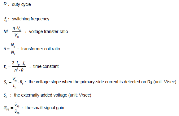
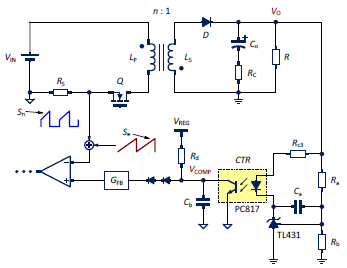
Figure 1. The schematic of the flyback converter with the TL431 and the optocoupler.
2. Power Circuit Small-Signal Model
Various small-signal models of flyback converters can be found in many references [1-3]. These models are all derived based on the method of state averaging. There are some minor differences among them, which probably result from the different assumptions being made. In this note, the small-signal model of Christophe Basso [1] is adapted for our feedback compensation design. However, with other small-signal models, similar results can also be achieved.
The transfer function of the continuous conduction mode (CCM)

This is a 1 pole 2 zeros system, as shown in Figure 2. The pole is determined by the circuit parameters and the size of the load. The first zero is fixed because it depends on the output capacitance and the equivalent series resistance (ESR). The other zero is on the right half s-plane, so called RHP zero. The location of RHP zero is determined by the input voltage, and the load current. Usually, in a well-designed system, the cross-over frequency is set far below the RHP zero frequency so the system can have sufficient phase margins. Based on this fact, this RHP zero is regarded as negligible when designing the compensation circuit.

Figure 2. The transfer function of CCM 1P2Z.
The transfer function of the discontinuous conduction mode (DCM)
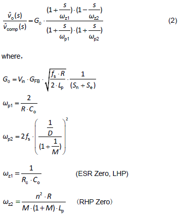
The transfer function of Equation (2) is shown in Figure 3. In small-signal model of discontinuous conduction mode, DCM, the power circuit has two poles and two zeros. One of the poles, ωp2, is extremely high (far above the target cross-over frequency). Therefore, designing the compensation, this pole can be neglected. As a result, with the small-signal model of either CCM or DCM, their transfer functions can be considered as 1 pole 2 zeros. Therefore, the selection of the feedback network becomes much easier.
From the transfer functions of Equation (1) and (2), some poles and zeros are fixed, such as the zero from the output capacitance and the equivalent series resistance ESR. However, most poles and zeros are influenced by the operating point, which describes the operating condition of the circuit and is specified by the input voltage and the load current condition. Next, the changes of the poles and zeros with the operating points will be illustrated with the circuit parameters plugged in.
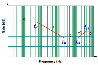
Figure 3. The transfer function of DCM 1P2Z.
Operating Points and Variations of Poles and Zeros
With a flyback converter as an example, given input voltage: 90V to 360V, load current: 0-3A, and output voltage as 12V. The circuit parameters are as below: LP = 1.1mH, NP/NS = n = 7.7, CO = 1360μF, RESR = 30 mΩ, RS = 0.56Ω, fS = 65kHz, Se = 3.46 x 10⁴ V/sec, GFB = 0.3333, where Se and GFB are provided by the controller IC。According to the operating principle of flyback converters, in a typical design, high input voltage with light load always causes converters to operate in continuous conduction mode; on the contrary, low input voltage with heavy load in the discontinuous conduction mode. A boundary exists between CCM and DCM, as shown in Figure 4 and its equation is as Equation (3).

Figure 4. The boundary of CCM and DCM.

The Variations of Poles and Zeros at Different Operating Points
Table 1 shows the DC gains and the locations of poles and zeros. Figure 5 shows the Bode plot for the different input voltages and load currents. From the plot, it is clear that the gain is higher with high line and light load. This helps in choosing the operating point as the criteria for feedback network design. It is better to design the feedback network under low line and heavy load condition. Adequate phase margin under such condition, can achieve an even better phase margin at different operating conditions.
Table 1. The DC gains and the locations of poles and zeros at different operating points
|
VIN (V)
|
90
|
180
|
270
|
360
|
90
|
90
|
90
|
360
|
360
|
360
|
|
IO (A)
|
3.0
|
3.0
|
3.0
|
3.0
|
3.0
|
2.0
|
1.0
|
3.0
|
2.0
|
1.0
|
|
Mode
|
CCM
|
CCM
|
CCM
|
DCM
|
CCM
|
CCM
|
DCM
|
DCM
|
DCM
|
DCM
|
|
G0 (dB)
|
13.1
|
16.5
|
17.0
|
17.1
|
13.1
|
15.6
|
17.0
|
17.1
|
18.8
|
21.8
|
|
fP1 (Hz)
|
59.0
|
53.0
|
57.0
|
58.5
|
59.0
|
44.0
|
19.5
|
58.5
|
39.0
|
19.5
|
|
fP2 (Hz)
|
NA
|
NA
|
NA
|
21.7k
|
NA
|
NA
|
25k
|
21.7k
|
32.6k
|
65k
|
|
fZ1 (Hz)
|
3.9k
|
3.9k
|
3.9k
|
3.9k
|
3.9k
|
3.9k
|
3.9k
|
3.9k
|
3.9k
|
3.9k
|
|
fZ2 (Hz)
|
16.5k
|
44.2k
|
75k
|
106k
|
16.5k
|
24.7k
|
49.5k
|
106k
|
160k
|
319k
|
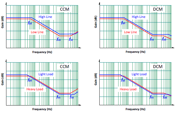
Figure 5. The variations of the gains vs. frequency with different operating conditions.
3. Feedback Compensation Circuit Design
From the previous analysis, poles and zeros vary with operating points as do low-frequency DC gains. There are many ways to design compensation circuits. Typically, a Type-II compensator (with one zero frequency pole, one low-frequency zero, and one pole) is most suitable in this case. Making a low-frequency zero to compensate the low-frequency pole and also making a high-frequency pole to compensate the ESR zero can achieve a better phase margin. A specific mid-band gain is chosen to get the proper cross-over frequency, and the system will therefore be stabilized.
One of the practical ways is setting a good “target loop gain” as

Such loop gain is just a straight line with the slope of -20dB/dec on the Bode plot as seen in Figure 6. At the low frequency or DC region, the gain is extremely high (equivalent to the open-loop gain of the compensator), so the theoretical adjustment rate of the DC regulating voltage can be set as zero. Its cross-over frequency, fC, is
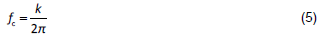
Since its slope is about -20dB/dec, its phase margin is about 90° near the cross-over frequency.
For an off-line flyback converter, it is best to set the cross-over frequency between 800Hz and 3kHz under the condition of low line and full load (where switching frequency is 65kHz).
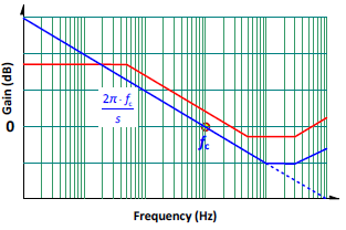
Figure 6. The transfer function of the power circuit (in red) and its target loop gain (in blue).
Design Procedure
As discussed above, any compensation method will work. The design procedures are listed below:
1.Design the compensation network under the condition of low line (input voltage) and full load. It usually will give a very good phase margin even at various conditions.
2.Set the cross-over frequency fC, and its loop gain as -20dB/dec in the Bode plot. Higher cross-over frequency means faster transient response. However, it is impossible to compensate RHP zero by the poles. Therefore, the cross-over frequency must be far below from RHP zero. Practically, the cross-over frequency is set below 3kHz.
3.Define a 2-pole-and-1-zero compensation circuit and set the zero as the low-frequency pole of the power circuit. Set the high-frequency pole as the ESR zero of the power circuit. Implement the design by a Type II compensator. Its transfer function can be the “target loop gain”.
4.Calculate mid-band gain according to power circuit gain at fC.
5.Estimate phase margin.
6.The transfer function of the compensation network is determined.
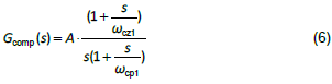
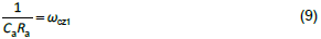
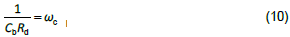
In other words, A、ωcp1 and ωcz1 in Equation (6) can be found.
Implementation of Compensator
1.This note illustrates the design method with a typical Type II circuit, a widely used circuit block of TL431 and the optocoupler, as shown in Figure 7.
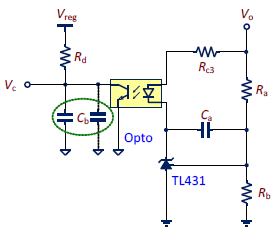
Figure 7. The schematic of the typical compensation circuit.
2.The small-signal transfer function of the circuit in Figure 7 is as shown below [5]:
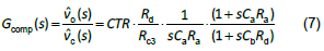
Figure 8 is its Bode plot.
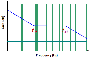
Figure 8. The Bode plot of the Type II compensation circuit
3.From Equation (7), there are 7 parameters, Ra、Rb、Rc3、Rd、Ca、Cb and CTR to be decided, and only three of them are known.
4.First, choose Rd. Most new controller IC’s have set the Rd value, which can be obtained from vendors.
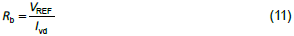
5.Next, the reference voltage VREF can also be obtained from vendors, typically 2.5V. To make TL431 function properly, the current through Rb (Ivd) must be at least 125μA. Ivd is usually specified as 250μA with some margins. Therefore, the values of Ra and Rb can be determined.

6.The current transfer ratio of the optocoupler (CTR) can be estimated according to the information provided by vendors. CTR is a nonlinear value, varying with the current through the optocoupler diode. Usually the current is on the order of hundreds μA with CTR around 0.1 to 0.5. The exact value can be found through the measurement. Here CTR is assumed to be 0.5.
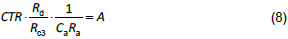
7.Now, four of the seven parameters are decided. The rest three can be calculated by Equation (8), (9) and (10).
8.RC3 acquired from Equation (8) must be evaluated. From how the TL431 works, the cathode voltage must be higher than 2.5V and the current through the cathode (Icathode) should be greater than 1mA to get a correct regulating voltage. Usually, a 1kΩ resistor will be added in shunt with the optocoupler diode to provide sufficient cathode current. This shunt resistor will not change the small signal model. Therefore, we can derive the following:

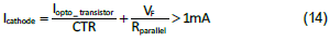
where VF is forwarded biased voltage drop of the optocoupler, around 1.0V. The maximum value of RC3 can then be estimated.
Assume Icathode is 1.5mA, and RC3 should be less than 5.6kΩ. Excessice RC3 will lower the mid-band gain. If RC3 is greater than the maximum value, the cross-over frequency will be set lower or another compensation method will be used.
9.There exists an equivalent capacitance, around 2nF to 5nF, in shunt with the phototransistor of the optocoupler. The total Cb value is this parasitic capacitance, which can be measured, and the external added capacitor. If the parasitic capacitance is dominant, then no external capacitance is needed. Since ESR zero cannot be compensated completely, the phase margin will become worse.
Design Tools and Simulation Verification
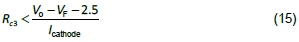
Two Mathcad computation procedures, Flyback CCM Type II Compensation” and “Flyback Loop Gain Analysis” have been used to facilitate the calculation and analysis of the feedback network design. Simplis simulations are used to compare errors of the simulation models. Figure 9 is the schematic of Simplis simulation circuit. Figure 10 to Figure 12 show the comparisons of Mathcad analysis and Simplis simulations. Figure 10 and Figure 11 are the Bode plots of the transfer functions of the power circuit and the compensation network, respectively. Figure 12 is the Bode plot of the closed-loop gain, (a) magnitude and (b) phase. Red lines indicate the results from Mathcad calculation and blue lines from Simplis.
From the low frequency to cross-over frequency, the small signal models match very well. The model starts to show a large mismatch at the high frequency region. However, since the loop gain is much less than 1, the mismatch can be neglected. Figure 13 shows the step response of the output voltage for the load current from 1A to 3A with 90V input voltage by Simplis simulation. Fairly small overshoot and settling time are shown.
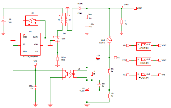
Figure 9. The schematic of the Simplis simulation circuit.
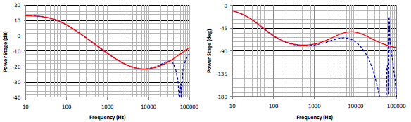
Figure 10. The Bode plot of the transfer function of the power circuit (a) magnitude, (b) phase.
Figure 11. The Bode plot of the transfer function of the compensation network (a) magnitude, (b) phase.

Figure 12. The Bode plot of the loop gain (a) magnitude, (b) phase.
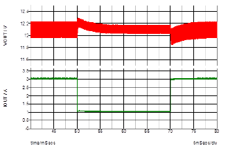
Figure 13. The response to a large step load current.
Reference
[1] Christophe P. Basso, “Switch-Mode Power Supplies Spice Simulations and Practical Designs”, McGraw_Hill, 2008.
[2] W. Kleebchampee and C. Bunlaksananusorn, “Modeling and Control Design of a Current-Mode Controlled Flyback Converter
with Optocoupler Feedback”, IEEE PEDS 2005.
[3] Yuri Panov and Milan M. Jovanovic´, “Small-Signal Analysis and Control Design of Isolated Power Supplies with Optocoupler
Feedback”, IEEE TRANSACTIONS ON POWER ELECTRONICS, JULY 2005.
[4] 王信雄, “定频返驰式转换器设计指南”, RTAD1202TC, 立锜科技设计指南, 2012.
[5] John Schönberger, ”Design of a TL431-Based Controller for a Flyback Converter”, Plexim GmbH.