Buck Converter Selection Criteria
Introduction
Richtek has a wide range of Step-Down DC/DC (Buck) converters,
but selecting the right Buck converter for your application can be a challenge.
This guide will help you to distinguish the different Buck converter types,
and highlights the key parameters which need to be considered for choosing the
optimal part for your application.
Buck converter basics
Buck converters are switch-mode step-down converters which
can provide high efficiency and high flexibility at higher VIN/VOUT
ratios and higher load current. The basic circuit is shown in Figure 1. Most
Buck converters contain an internal high-side MOSFET Q1 and low-side synchronous
rectifier MOSFET Q2, which are in turn switched on and off via internal duty-cycle
control circuit to regulate the average output voltage. The switching waveform
is filtered via an external LC filter stage. A feedback loop senses the output
voltage and controls the duty-cycle of the high-side MOSFET, thereby regulating
the output voltage. Asynchronous parts do not have an internal low-side MOSFET,
and need an external Schottky diode from switch node to ground.
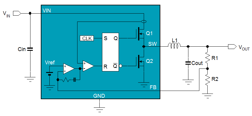
Figure 1. Buck converter basic circuit
Due to the fact that the MOSFETs are either ON or OFF,
they dissipate very little power, and the duty-cycle control makes large VIN/VOUT
ratios possible. The internal MOSFETs RDS(ON) mainly determines the
current handling capabilities of the Buck converter, and the MOSFET voltage
ratings determine the maximum input voltage.
Voltage and current rating selection
Application input voltage
When choosing a Buck converter, the input voltage range
is the first parameter that needs to be considered. Richtek Buck converters
can be divided in three main groups:
·
LV Buck with VIN range from 2.5V ~ 5.5V
·
18V HV Buck with VIN range from 4.5V ~ 18V
·
HV range with VIN range 4.5V up to 36V.
Many parts in the LV buck converter range are optimized
for running off single cell Li-Ion batteries, but can also be used for supplies
running from 5V rails.
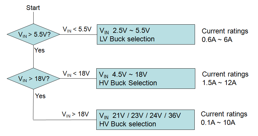
Figure 2. Richtek Buck converter selection flow
The 18V rated parts are normally used for applications
that run from 12V supply rails, but their wide voltage range makes it possible
to run them from 5V rails as well.
The 21V / 23V / 24V and 36V parts have a very wide application
range. Quite often these parts are selected when the input voltage rail has
a wide tolerance, or when it has voltage peaks and dips that the Buck converter
needs to be able to handle. The 36V parts are often used in applications that
need to run from industrial supply voltage rails like 24Vdc, or 13.5V car battery
powered automotive applications with high supply voltage surge.
Application current consumption
When considering the Buck converter current rating, there
are two factors to consider: The application average current consumption and
the application peak current.
The application average current should always be lower
than the device rated current as mentioned in the datasheet. How much lower
depends on the device power dissipation and application thermal conditions.
The application average current will determine the average heat in switching
MOSFETs which is related to conduction losses and switching losses. Conduction
losses are related to the internal MOSFET RDS(ON) : The MOSFET conduction
losses are I2 * RDS(ON). When the high-side and low-side
RDS(ON) are not the same, the application step-down ratio should
also be considered to check the power dissipation in high-side and low-side
MOSFETs. Switching losses are mostly related to the current, the input voltage
and the switching frequency. In most standard applications, the switching losses
are roughly 30% of the total losses, but in applications with higher input voltage
or high frequency, the switching losses can increase considerably. The application
total power losses can be derived from the datasheet efficiency curve:
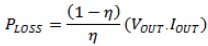 .
Please note that this power losses includes the inductor losses as well, which
are normally around 10% ~ 20% of the total losses. The IC maximum allowed power
dissipation depends on the IC package, the layout and the application maximum
ambient temperature. Layouts with more copper connected to IC pins and package
thermal pad can be helpful dissipate more power.
.
Please note that this power losses includes the inductor losses as well, which
are normally around 10% ~ 20% of the total losses. The IC maximum allowed power
dissipation depends on the IC package, the layout and the application maximum
ambient temperature. Layouts with more copper connected to IC pins and package
thermal pad can be helpful dissipate more power.
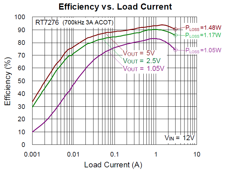
Figure 3. Efficiency curves at different output voltages
The application maximum current can normally be at the
same level as the device rated current as mentioned in the datasheet, sometimes
even a bit higher. The designer should make sure that the over-current protection
(OCP) is never triggered during maximum application load current. Buck converters
sense the inductor peak current (or valley current in some ACOT®
devices), and datasheet OCP current values refer to these inductor peak or valley
current levels. The difference between load current and inductor peak or valley
current is ½ the inductor ripple current, so be sure to include this
when checking the application maximum load current in relation to OCP current
levels.
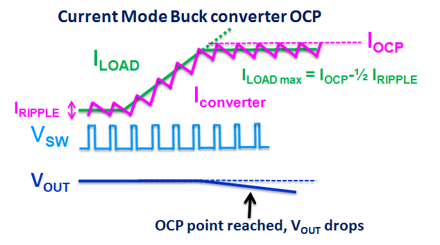
Figure 4. Buck converter over-current protection
Light load efficiency (PSM / Force-PWM selection)
For supply rails that need to be active in low power standby
modes, it is desirable to make the Buck converter efficiency at light load as
high as possible. Force-PWM* Buck converters keep the switching frequency fixed
over the entire load range. The high switching frequency at light load will
mean that the majority of losses at light load will be caused by switching losses.
Buck converters with enhanced light load efficiency will
reduce their switching frequency at light load; this is often called Pulse Skip
Mode (PSM**). The operation principle is as following: When the load reduces,
the inductor current valley reaches zero current at a certain point. Force-PWM
parts keep the low-side MOSFET conducting, which will make the inductor current
going negative. In PSM parts, the low-side MOSFET is switched off when the inductor
current reaches zero, and the switch node floats until the next time the high-side
MOSFET is switched on. The minimum ON time of the high-side MOSFET determines
the inductor peak current and average inductor current can only be reduced by
reducing the switching frequency; i.e. by inhibiting the internal clock, thereby ‘skipping
pulses’. Voltage regulation in PSM is accomplished by comparing the output
voltage ripple valley with the internal reference. PSM will reduce the converter
switching frequency to very low values at light load; down to a few kHz. This
reduces switching losses, thereby increasing the light load efficiency considerably.
PSM does have some disadvantages:
·
The output ripple voltage is a low frequency triangular waveform which
can be hard to filter. Depending on PSM regulation criteria and component values,
the PSM output voltage ripple amplitude can be higher than in PWM mode. Some
loads may be sensitive to this.
·
When a converter running in PSM suddenly sees a load step, it quickly
has to switch from PSM to PWM mode. This transition will result in larger output
voltage undershoots compared to converters that always run in force-PWM mode.
·
In PSM, the regulated average voltage is slightly higher (~1%) compared
to PWM mode.
·
Due to the variable switching frequency, PSM can sometimes cause interference
in sensitive adjacent circuits
If the application does not need enhanced light load efficiency,
it is better to select Force-PWM parts, which will provide stable operation
conditions over the full load range.
*In some Richtek documents, Force-PWM mode is called PWM
mode or Continuous Operation Mode.
** In some Richtek documents the Pulse Skip Mode is called PWM/PSM or DEM or
Discontinuous Operation Mode.
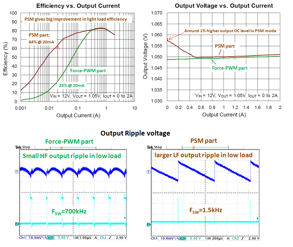
Figure 5. PSM advantages and disadvantages
Switching Frequency considerations
The switching frequency of Buck converters is important
parameter to consider. Higher switching frequency makes it possible to use smaller
inductor and capacitors, and improves the step load behaviour of the converter.
However, it also increases switching losses and extends the EMI radiation frequency
range. Higher switching frequency can also limit the maximum step-down ratio
that can be achieved: The minimum duty-cycle is limited by the converter minimum
ON time and the frequency:

For example, at a given tON(MIN) = 100nsec,
a 1.2MHz converter has a minimum duty-cycle of 12%, and would not be able to
step down from 12V to 1.2V. An 800kHz converter would have a minimum duty-cycle
of 8% and can step-down 12V to 1.2V.
Very high frequency Buck converters (> 1MHz ) are often
used when the input voltage is relatively low; (5V or lower) because the switching
losses at low VIN are lower, and the maximum step down ratios for
these applications are lower as well.
For most 12V applications, switching frequencies between
500kHz ~ 800kHz are suitable, providing a good compromise between switching
losses and component size.
In high current applications with higher input voltages
(>18V) it is better to use switching frequencies lower than 500kHz to reduce
the switching losses and still allow high step-down ratios.
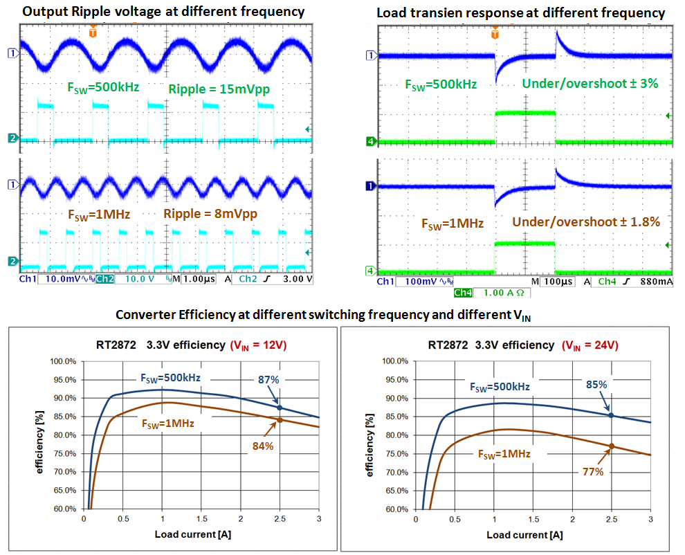
Figure 6. Buck converter switching frequency influence
on ripple, transient response and efficiency
Buck converter control topology selection criteria
The Richtek DC/DC portfolio contains a wide range of Buck
converters with different control topologies, including Current Mode (CM), Current
Mode-Constant On Time (CMCOT) and Advanced Constant On Time (ACOT®)
control topologies. Each topology has its advantages and drawbacks, so when
selecting a Buck converter for an application, it is good to understand the
characteristics of each topology.
Current Mode control
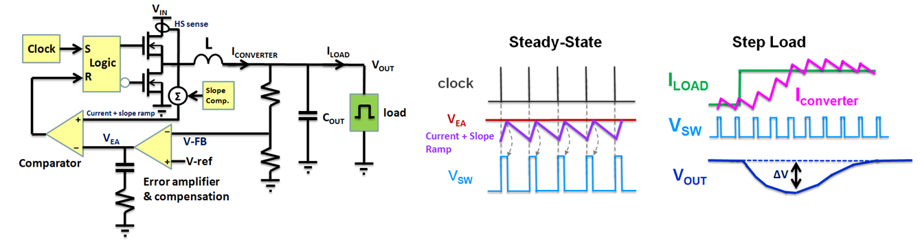
Figure 7. CM Buck converter basic circuit diagram and
operation waveforms
Current Mode converters have an internal clock generator,
an error amplifier and current sense. The error signal is compared with the
sensed peak current and controls the on time of the upper MOSFET. The start
of a new switching cycle is determined by the clock signal, so the system runs
in fixed switching frequency. Control bandwidth is usually around 1/10th
of the switching frequency.
|
Current mode Buck converter
|
|
Advantages :
- Fixed frequency operation
- Can be Synchronized to ext. clock
- Established technology
- Stable with MLCC
|
Disadvantages :
- Slow response to fast load steps
- Needs error amplifier compensation
- Needs slope compensation
|
If the application load current is relatively steady, you
can use current mode Buck converters. If the system is susceptible to noise
at certain frequencies, you also may want to use a current mode Buck converter,
and maybe synchronize it to an external clock signal to set the switching frequency
very precisely. Many current mode Buck converters in the LV input range support
100% duty-cycle operation, which makes it possible to run these Buck converters
at VIN very close or equal to VOUT.
Current Mode - Constant On Time control
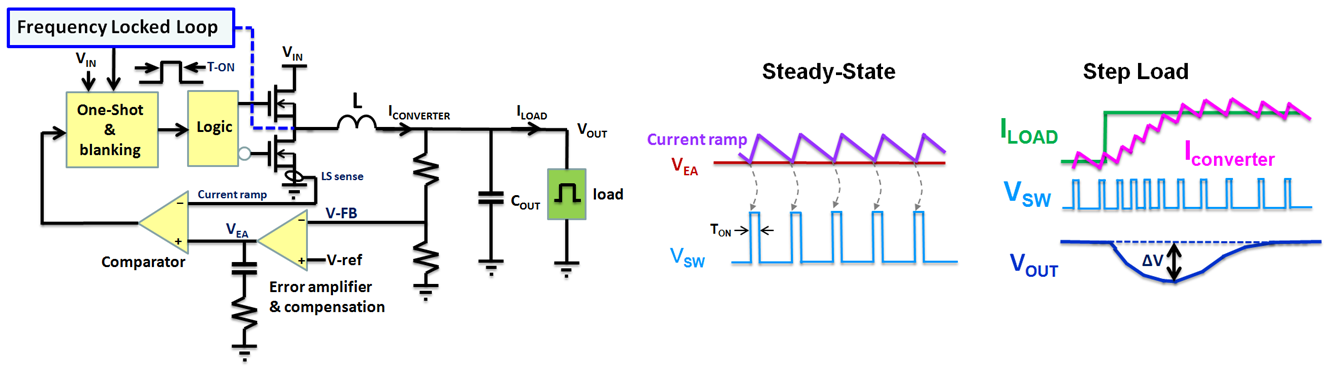
Figure 8. CMCOT Buck converter circuit diagram and operation
waveforms
CMCOT Buck converters do not have an internal clock; the
upper MOSFET always conducts for a pre-defined fixed ON time. The duty-cycle
is regulated by changing the OFF time of the upper MOSFET. CMCOT converters
also contain a current sense and error amplifier, but now the falling slope
of the current is compared to the output of the error amplifier. The fact that
the system does not need to wait for a next clock-cycle makes it possible to
react more quickly to sudden step loads; as soon as the output voltage drops
and the error amplifier voltage rises above the falling current slope, a new
ON time is triggered and the inductor converter current rises again.
|
Richtek Current Mode-COT (CMCOT) Buck converter
|
|
Advantages:
- Fast response to load steps
- Low Side current sense
- Small minimum ON time allows small duty-cycles.
- Constant average frequency
- Stable with MLCC
- Does not need slope compensation
|
Disadvantages:
- Needs error amplifier compensation
- Cannot be Synchronized to ext. clock
- Some frequency deviation during load transients.
|
If the application load has moderate transient load conditions,
you may want to choose a CMCOT topology Buck converter, to reduce output voltage
fluctuation during load transients. CMCOT converters can achieve 20 ~ 30% better
load transient behavior when compared to standard current mode Buck converters.
CMCOT also is less sensitive to noise in low duty-cycle applications. Due to
its very small minimum ON time, the CMCOT Buck converter can be used for applications
with larger step-down ratios. CMCOT converter switching frequency will show
some deviation during load transients.
Advanced Constant On Time control (ACOT®)
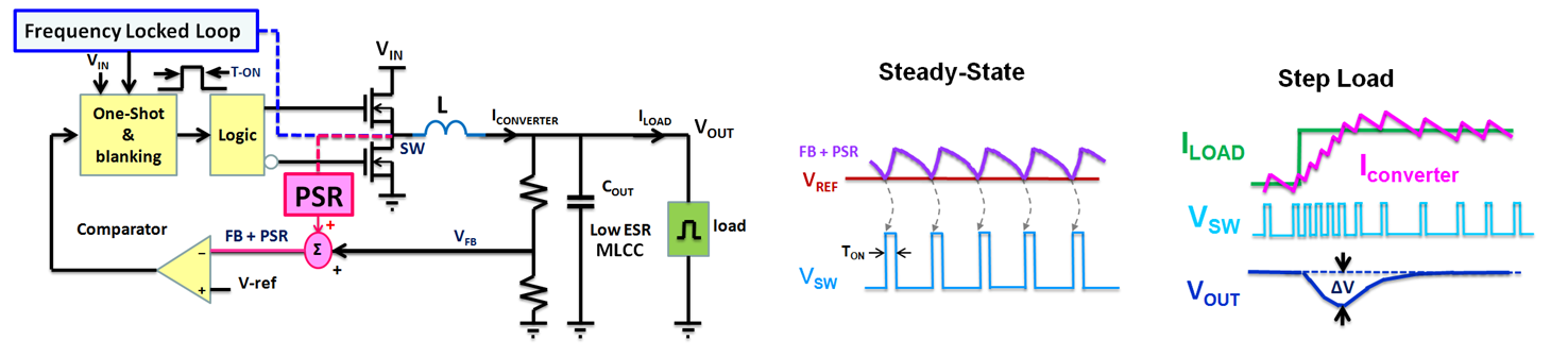
Figure 9. CMCOT Buck converter circuit diagram and operation
waveforms
ACOT converters do not contain an error amplifier or
current sense; they directly compare the feedback signal (DC level + ripple
voltage) with an internal reference. When the feedback signal falls below the
reference, a new fixed ON time is generated and inductor current rises. If the
output voltage has not recovered, another ON time is generated after a short
blanking period until the inductor current matches the load current and output
voltage is at its nominal level again. To make the converter stable with low
ESR ceramic output capacitors, an internally generated Pulse Shaping Regulator
(PSR) ramp signal is added to the ripple and the DC level from the converter
output. These are summed and then compared with an internal reference. When
this summed voltage drops below the reference, the comparator triggers the ON
time generator.
A sudden drop in output voltage will immediately result
in a new ON time, and the converter can generate successive ON times as long
as the output voltage has not recovered. This makes the ACOT topology reaction
speed to load transients extremely fast.
A special frequency locked loop system will slowly adjust
the ON time to regulate the average switching frequency to a defined value.
|
Richtek Advanced-COT (ACOT®)
Buck converter
|
|
Advantages:
- Extremely fast response to load steps
- Does not need current sense
- Small minimum ON time allows small duty-cycles.
- Constant average frequency
- Stable with MLCC
- Does not need slope compensation
|
Disadvantages:
- Cannot be Synchronized to ext. clock
- Large FSW deviation during dynamic load
|
If the application load shows severe fast load transients
(like seen in Core and DDR rails) it is best to choose ACOT Buck converters,
which can improve load transient behavior by a factor 2 to 4, and make it possible
to use smaller output capacitors. They are especially suitable for low duty-cycle
applications. Due to their very small minimum ON time, ACOT Buck converters
with high switching frequencies can be used in applications with large step-down
ratios. ACOT converter switching frequency can show considerable deviation during
load transients. But the absence of loop compensation and slope compensation
and the extremely fast loop response makes ACOT designs simple, flexible and
cost effective.
Other Buck converter selection criteria
External soft-start
All Richtek Buck converters have a soft-start function.
After enabling the converter, the duty-cycle is gradually increased to allow
a smooth rising output voltage, which avoids inrush current due to sudden charging
of the output capacitors. Converters with internal soft-start have a fixed soft-start
time. If the application uses very large output capacitance or requires a specific
soft-start time, it is better to select a converter with externally programmable
soft-start; the soft-start time can be set by an external capacitor.
External compensation
Current mode converters need error amplifier compensation
to ensure stable operation. The type-II compensation components determine the
converter bandwidth and the phase boost frequency. Converters with external
compensation have more flexibility in setting the desired bandwidth and phase
margin with different types of output capacitors over a wider range of input
and output voltage conditions.
Programmable frequency
Some converters have a programmable frequency function:
The switching frequency can be set by means of an external resistor.
This gives more flexibility in choosing the best switching frequency for the
application; higher frequency to reduce ripple or component size or get better
transient behavior, or lower frequency to improve efficiency or reduce higher
harmonics.
External sync input
Some current mode converters have an external sync input
that allows the internal clock to be synchronized to an external clock signal.
This makes it possible to set the switching frequency at a very precise value
(for avoiding noise at sensitive frequency bands), and also make it possible
to run several converters at the same frequency.
Low-Dropout mode or 100% duty-cycle mode
Many current mode Buck converters from the LV series
have Low Dropout mode function: When the input voltage drops, these Buck converters
gradually increase the duty-cycle and will continuously switch-on the high side
MOSFET when the input voltage drops below the regulated output voltage. This
function is especially suitable in battery powered applications, and can extend
application operation time when the battery is almost depleted.
Power Good function:
The Power Good function will monitor the Buck converter
output signal and provide a means of telling the system when the output voltage
is within a certain operating range. Power Good can be used for system initialization,
fault detection or start-up sequence.
Over Current Protection:
All Richtek Buck converters have Over Current Protection
(OCP). When the inductor current exceeds the OCP level, the converter duty-cycle
is limited. Further load increase will result in output voltage drop. However,
there are different ways how the system behaves in overload condition:
·
Latch mode OCP: When during overload the output voltage drops below the
Under Voltage Protection (UVP) point, the system shuts down and latches. The
converter needs to be re-enabled or cycle the input voltage for restart. This
protection ensures zero power after overload, but does not have auto restart.
·
Hiccup mode OCP: When during overload the output voltage drops below
the UVP point, the system shuts down and initiates a restart with soft-start.
Continuous overload will show continuous shut-down/restart cycle or hiccup mode.
The advantage of hiccup mode is low average overload current, and guarantees
auto restart after the overload is removed.
·
Non UVP: During overload the output voltage drops, but there is no UVP
action. The system continues to run at OCP current level during overload. The
output voltage recovers immediately after the overload is removed. But the continuous
OCP current level can lead to increased temperature in longer term overload
conditions.
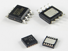
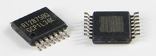
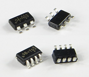
IC package selection considerations
Richtek Buck converters are available in many types
of packages: from tiny CSP 1.3x2.1mm to cost effective TSOT-23-6 to larger TSSOP-14
thermally enhanced package.

Figure 10. Various IC packages used in Richtek Buck converters
Which IC package is most suitable for your application
depends on a number of factors:
 In
applications that are extremely limited in height and PCB space (i.e. mobile
phones and tablet PCs or other small portable devices) you will most likely
select CSP packages. For these packages, multi-layer PCB layouts are required,
and they need more precise placement and well controlled soldering process.
In
applications that are extremely limited in height and PCB space (i.e. mobile
phones and tablet PCs or other small portable devices) you will most likely
select CSP packages. For these packages, multi-layer PCB layouts are required,
and they need more precise placement and well controlled soldering process.
SOP-8 (exposed pad) and DFN2x2 and DFN3x3 packages are
often used in Buck converters: Their pin count ranges from 6 ~ 12 pins for extra
functionality, and they offer good thermal performance due to exposed thermal
pad. They are cost effective, making them a popular choice for many applications.
It is possible to use these parts in single sided layout, but for better thermal
and electrical performance multi-layer PCB layouts are recommended.
 Larger
packages like TSSOP-14 or WDFN-14L 4x3 have larger thermal pads, which allow
them to dissipate more power. It is important to connect the thermal pad to
large PCB copper area, and use vias to inner layers to enhance the PCB cooling
properties.
Larger
packages like TSSOP-14 or WDFN-14L 4x3 have larger thermal pads, which allow
them to dissipate more power. It is important to connect the thermal pad to
large PCB copper area, and use vias to inner layers to enhance the PCB cooling
properties.
 For
lowest cost solutions, TSOT-23-6 and SOT-23-8 packages are a good choice. The
6-pin packages are sufficient for the basic Buck converter, while the 8-pin
packages offer some extra functionality like soft-start or Power good. These
packages have no thermal pad, so most of the IC heat dissipation must be removed
through thermal flow via the package pins to the PCB copper. There are two different
die assembly structures: traditional wire-bonding and flip-chip. The key advantages
of a flip-chip package are better electrical performance and improved thermal
capabilities compared to conventional wire-bonded products.
For
lowest cost solutions, TSOT-23-6 and SOT-23-8 packages are a good choice. The
6-pin packages are sufficient for the basic Buck converter, while the 8-pin
packages offer some extra functionality like soft-start or Power good. These
packages have no thermal pad, so most of the IC heat dissipation must be removed
through thermal flow via the package pins to the PCB copper. There are two different
die assembly structures: traditional wire-bonding and flip-chip. The key advantages
of a flip-chip package are better electrical performance and improved thermal
capabilities compared to conventional wire-bonded products.
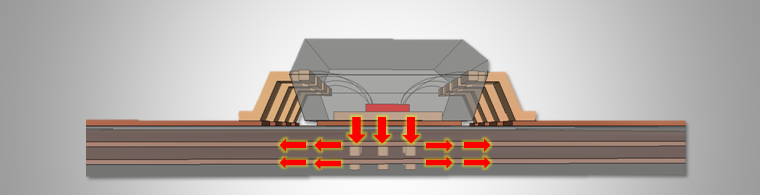
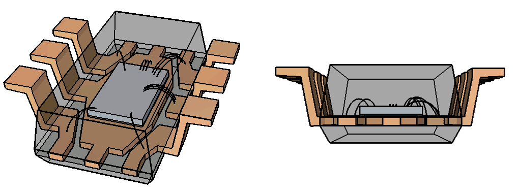
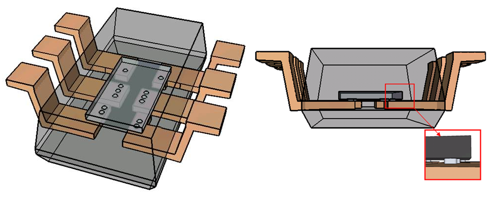
Overview for conventional wire-bond vs. flip-chip on lead
in TSOT-23-6 package:
|
Wire bonding:
|
Flip-Chip:
|
|
|
|
|
The silicon die is glued to the center (GND) lead,
and the die electrical connections are wired to the lead frame pins
via bonding wires, which are typically 25-38um gold or copper wires.
|
The topside of silicon die is mounted via pillar
bonding to the lead frame providing both the thermal and electrical
connections directly from silicon die to the lead frame.
|
|
Electrical performance differences:
|
|
The thin wires add resistance, inductance and stray
capacitance to critical circuit nodes, which reduces the performance
of high frequency switching converters.
|
The short interconnect length of pillar bonding
delivers significantly less resistance, inductance and stray capacitance,
which minimizing I2R and switching losses while reducing waste heat.
|
|
Thermal performance differences:
|
|
The bonding wires are poor heat conductors so most
of the potential heat transfer of the pins is lost. Heat transfer is
mostly from the back side of the die through adhesive to the center
ground pin, causing a hot spot on the center pin.
|
All pins are acting as small heat sinks and can
be used for efficient cooling, so there is more heat transfer from package
to PCB, resulting in lower die temperature.
|
 Buck
converters with higher current capabilities (≥ 6A) often make use of flip-chip
technology as well, to avoid the extra resistance of the bonding wires. These
parts make use of UQFN packages with special lead frames for optimal connection
to the silicon die in order to minimize the total RDS(ON). For optimal
package cooling, it is key that the PCB layout has sufficient copper to the
IC pin connections, with thermal vias to inner layers for increasing the heat-sinking
effect of the PCB.
Buck
converters with higher current capabilities (≥ 6A) often make use of flip-chip
technology as well, to avoid the extra resistance of the bonding wires. These
parts make use of UQFN packages with special lead frames for optimal connection
to the silicon die in order to minimize the total RDS(ON). For optimal
package cooling, it is key that the PCB layout has sufficient copper to the
IC pin connections, with thermal vias to inner layers for increasing the heat-sinking
effect of the PCB.
In Richtek datasheets, flip-chip packages have a designator “F”
at the end of the full part-number.