1.Introduction
Longer battery life and shorter charging times are some of the challenges in battery management in modern hand-held applications like Smart-Phones, Tablet PCs, POS and other portable equipment.
Devices with powerful processors are more power hungry and require larger capacity batteries to guarantee battery life. To quickly charge large capacity batteries, powerful high current chargers are needed. Linear chargers have too limited charge current capability for this purpose, so switching charger topology has to be adopted. This application note explains several application aspects of switching chargers for single cell Li-Ion batteries and introduces three switching chargers from the Richtek Li-Ion charger portfolio: RT9458 (1.55A), RT9460 (3A) and RT9466 (5A).
2.Li-Ion battery charging
Charging Li-Ion cells needs special care, as wrong charging can shorten battery life, or damage the battery and lead to unsafe conditions. Figure 1 below shows the typical Li-Ion charge cycle.
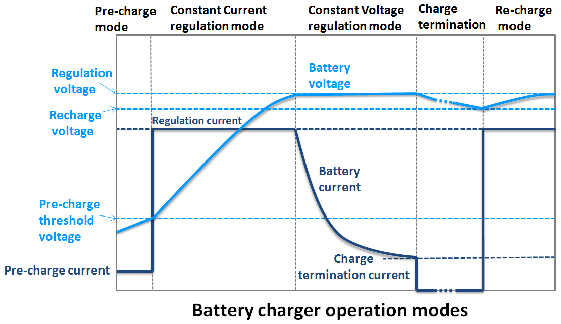
Figure 1
Li-Ion batteries that have been deeply discharged normally require some pre-conditioning: Below a certain battery voltage, the battery charger will first provide a low pre-charge current to pre-condition the battery for normal charging. This pre-conditioning can also reset the battery internal under-voltage protection. In normal use, the pre-charge cycle will not be used, as most applications will not allow deep discharge of the battery.
When the battery voltage exceeds the pre-charge level, the charger goes to fast charging mode. In this mode the charger delivers a pre-defined constant current (CC), which is normally related to the battery cell capacity. Most Li-Ion applications can fast-charge with currents between 0.5C and 1C (where C is the battery capacity in Ah). Batteries with lower internal impedance can use higher charging current. High current Lithium-Polymer (Li-Po) batteries (i.e. the types used in drones) use special battery construction and can accept higher charge rates like 2C~4C.
When the battery voltage reaches the battery regulation voltage, the charger will switch from constant current to constant voltage (CV) mode, and the charge current slowly decays. The maximum CV regulation voltage needs to be accurately controlled to prevent over-charge and potential battery damage. Li-Ion batteries CV level varies between 4.15 to 4.4V. Most Li-Ion batteries are considered fully charged when the battery voltage is at its regulation voltage and charging current has dropped below 5% of rated charge current. At this point charging is terminated. It is not recommended to continuously trickle charge Li-Ion cells, as this will reduce battery life. Most chargers will start a re-charge cycle when the battery voltage drops below a certain level (often around 3.9V or 4.0V)
From the above it is clear that Li-Ion battery chargers need to have accurate battery voltage sensing and separate control loops for constant output current and constant output voltage. Switching chargers can be used for a wide range of batteries, which means that many charging control parameters need to be adjustable. The most convenient way to do this is via I2C control.
3.Challenges in fast charging Li-Ion cells
In many battery charging applications, there are practical reasons that will limit the ideal charging condition of a battery. Figure 2 illustrates this.
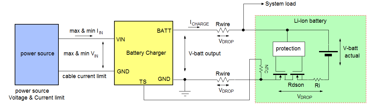
Figure 2
· The input supply may not be able to provide the required input current and voltage that the battery charger needs in order to optimally charge the battery in fast charge condition. This is especially true when the input power is taken from a USB port with limited current capability.
· When charging current becomes higher, the total resistance between charger and battery (PCB trace, connector, protection MOSFET Rdson and battery Ri) will cause a voltage drop. This will result in an error between the actual battery voltage and the sensed battery voltage.
· Fast charging will heat-up the battery. Most battery chargers will sense the battery temperature and charging current and/or charge voltage will be reduced at elevated battery temperatures to avoid overheating.
· Increased system load may reduce the battery charging current when the system power + battery charge power exceeds the input power limit.
4.Switching charger application & special functions
A typical switching charger application is shown in figure 3
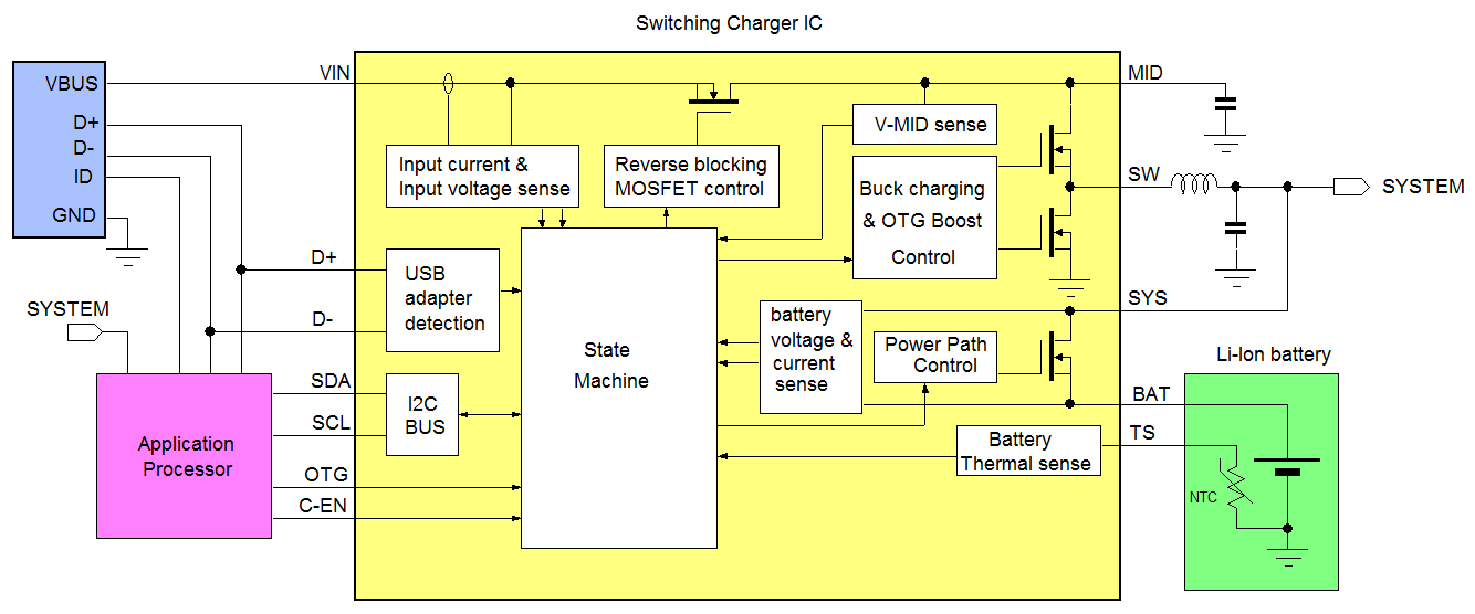
Figure 3
The input supply for a switching charger IC often comes from a USB port. The switching charger is basically a Buck converter with voltage and current control loops which steps down the VBUS supply to a suitable voltage for system supply and battery charging. Most applications will have an application processor which detects the attached USB port capabilities and sets the charging conditions based on the input capabilities and the battery type that is used. The switching charger contains many control functions for battery charging and input current and voltage control. The following section describes some of the special functions of switching chargers to deal with input USB compatibility and optimizing battery charge conditions.
Average Input Current Regulation (AICR)
Most switching chargers implement an Average Input Current Regulation loop. This control loop will adjust the charge current in such a way that the charger input current will not exceed a certain level. The input current level can be set via I2C based on the input source current capability, or via automatic (USB) charge port detection. The input current of switching chargers is defined by: 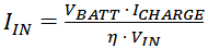 where η is the charger efficiency. So in AICR mode, the battery fast-charge current will drop as the battery voltage rises.
Minimum Input Voltage Regulation (MIVR)
Since it is not always clear what kind of power source is connected, it could happen that the charger draws too much current from the power source, which could overload the power source. To avoid this, a minimum input voltage control loop can be activated which monitors the charger input voltage and reduces the battery charge current when the input voltage drops below a certain level. For charging from USB ports, the MIVR level could be set at 4.5V, to ensure that the USB port is not overloaded.
USB charging port detection via D+ & D- pins
The default USB 2.0 ports can only provide 500mA of current, so when charging from a default USB port, the charger input current should stay below 500mA to avoid overloading the port. Most switching chargers will start working in AICR 500mA mode in default start-up condition for this reason. To accommodate higher currents over USB, the USB Battery Charging standard BC1.2 defines a method to communicate the power capabilities of a USB port, making use of the D+ and D- data lines. The BC1.2 standard defines 3 types of ports:
· Standard Downstream Port (SDP) (host D+ and D- each have 15k resistor to GND)
· Dedicated Charging Port (DCP) (host D+ and D- are connected together)
· Charging Downstream Port (CDP) (host includes some logic which handshakes with detection circuit)
SDP can only provide 500mA current, whereas DCP and CDP can provide at least 1.5A current. A DCP is not able to transfer data over the D+ and D- lines, but a CDP can use the D+ and D- lines for data transfer.
Besides BC1.2 standard, there are also some brand-specific D+/D- configurations that can be recognized by the charger IC, like Apple, Samsung, Sony, Nikon adapters, which use specific resistor dividers at D+ and D- for identification.
The charger IC will check the host D+ and D- lines during start-up and determines what kind of host port is connected. It then can configure the AICR current level to match the connected USB port or adapter capabilities.
IR compensation function
As was shown in figure 2, the resistance from charger output to battery including PCB trace resistance, battery connector resistance, battery protection MOSFETS Rdson and battery internal resistance will cause voltage drop between charger IC V-battery sense pin and actual battery voltage. This effect becomes more pronounced at higher charging currents, and will result in prematurely entering the CV charging mode. The resulting effect is a prolonged CV charging cycle, which increases the total charging time. This behavior is illustrated in figure 4.
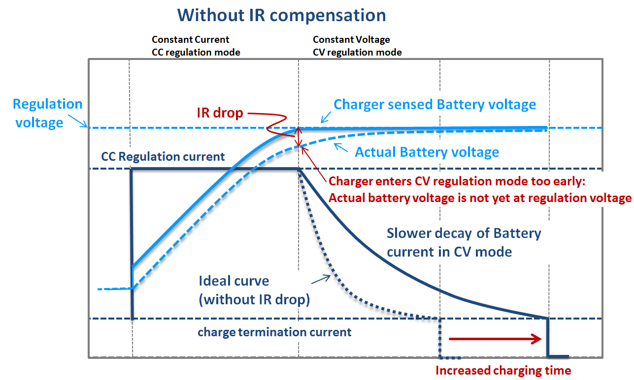
Figure 4
To compensate the IR drop, some switching chargers have programmable IR compensation, which makes it possible to add a current dependent compensation factor to the charger IC battery voltage sense, based on the total resistance between charger IC and battery. An example charging curve with IR compensation is shown in figure 5.
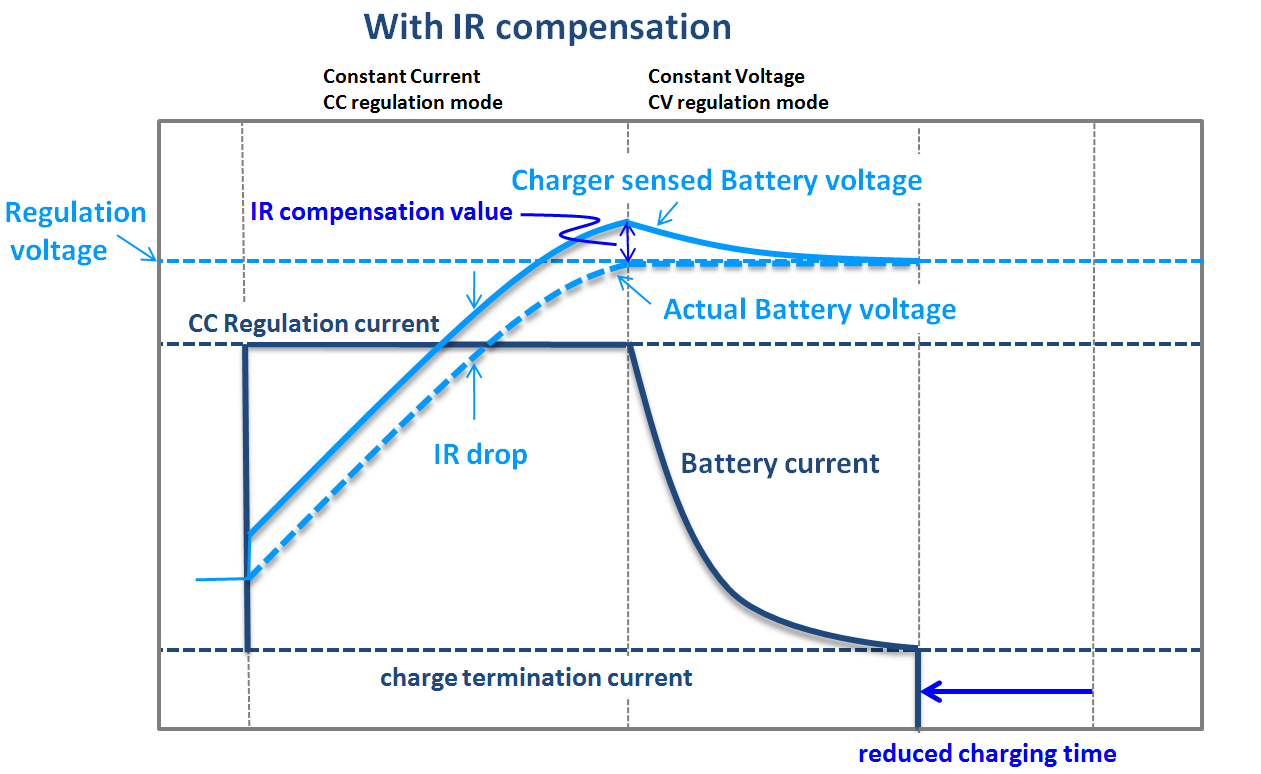
Figure 5
Battery charging at different battery temperatures
Most switching chargers will follow JEITA guidelines for charging conditions of Li-Ion batteries at various battery temperatures. JEITA guidelines define 5 temperature ranges in which different charging conditions apply: Cold, Cool, Normal, Warm and Hot. In cold and hot range, no charging is allowed. In cool and warm conditions, it is recommended to reduce either charge current or charge voltage or reduce both. In normal temperature range, charge voltage and current can be kept at nominal values. See figure 6.
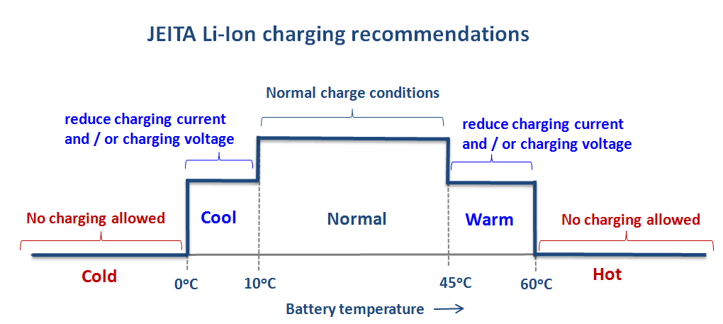
Figure 6
|
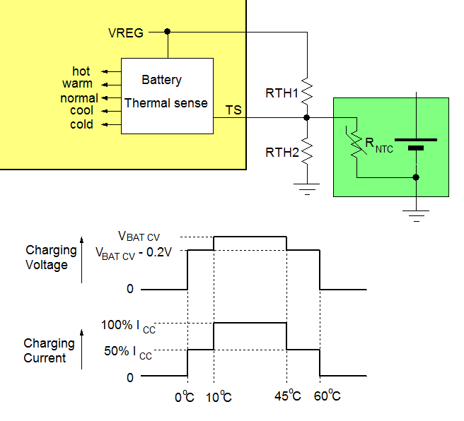
Figure 7
|
The temperature ranges are sensed by the charger IC by connecting the battery NTC to a resistor divider which is biased from the IC reference voltage. The values for RTH1 and RTH2 can be selected to match the IC V-TS cold and hot thresholds at 0oC and 60oC based on the NTC type used. The charger IC will automatically change the charging conditions in cool and warm ranges, and suspend charging in cold and hot condition. Most charger ICs allow programmable changes in charge conditions in cool and warm temperature range.
Figure 7 shows the battery temperature sense application and an example of different battery charge current and charge voltage at different temperature ranges.
|
Automatic Power Path function
Switching chargers with Automatic Power Path function have the ability to select what power source is used for supplying system power. Figure 8 shows a condition where the charging adapter is connected, and battery is being charged while the system is also being powered. The Power Path MOSFET is switched on, and the Buck stage provides the system load current and the requested battery charging current, as long as the input supply has the capability to provide sufficient IIN to accommodate this. If the total requested input current exceeds the AICR limit, the charger will reduce the battery charging current to guarantee the requested system current and keep the input current below AICR limit.
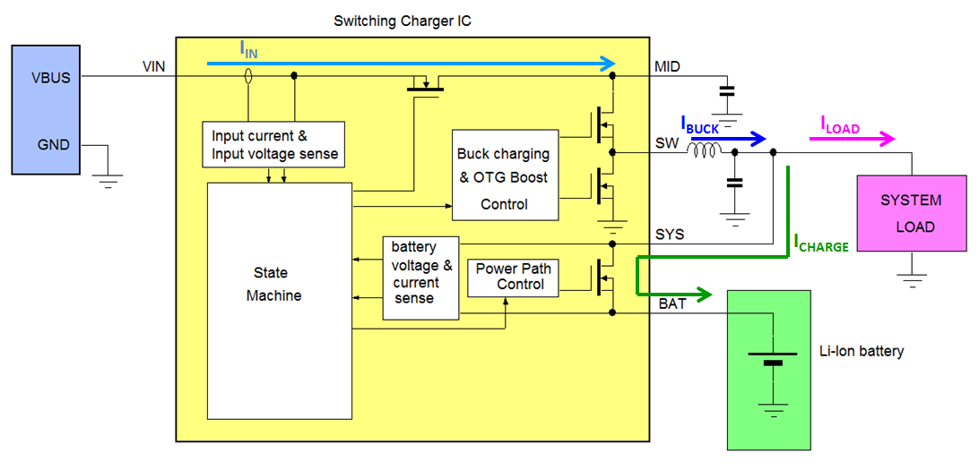
Figure 8: charger provides both system load and battery charge current
In extreme system load cases, the battery current can even reverse, where both adapter and battery can deliver the system load. (Figure 9)
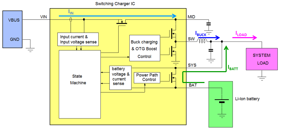
Figure 9: system load provided by charger and battery
The power path control MOSFET will be switched off when the battery is fully charged, and this case only the adapter is providing the system load power. (Figure 10). Some chargers have a factory mode where the charger provides a regulated system voltage when no battery is attached.
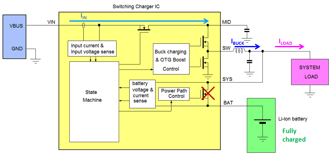
Figure 10: battery fully charged: charger provides system load.
When the adapter is removed, the power path control MOSFET will be switched on again and the battery will automatically supply the system load. The blocking MOSFET in the VIN line will be switched off. (Figure 11)
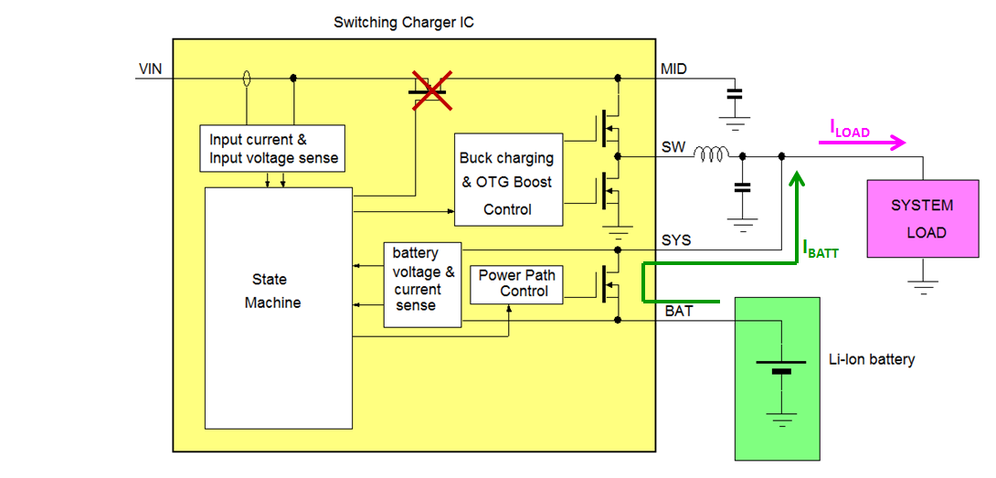
Figure 11: charger without input power, battery provides system load
If the device is not going to be used for a long time (i.e. during shipping) some chargers can set a shipping mode where the power path control MOSFET is switched off completely, also when no input power is provided. In this mode, battery leakage is minimized. Shipping mode can be reset by applying input power or I2C command. See figure 12.
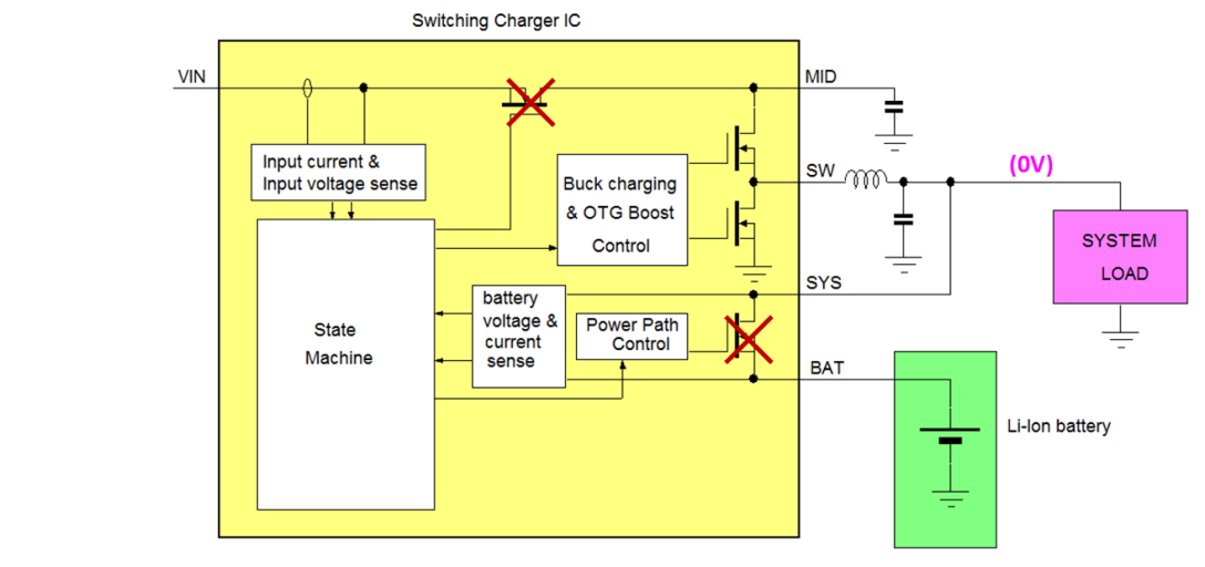
Figure 12: Charger in shipping mode, minimal battery leakage
USB On The Go (OTG) function
Many portable devices have a USB port with multiple roles: The port can serve as charging input when an adapter is connected to it; it can serve as a host USB port for connection of external slave devices like flash drives, digital camera, mouse or keyboard; but it can also be connected to a PC for data exchange. It means that the USB port sometimes serves as power input during charging, but in some cases it needs to supply power to external slave devices, or it can act as a slave itself. USB On-The-Go (OTG) defines these different operation modes, making use of the ID pin in Mini and Micro USB connectors, which identifies a certain device as host or slave. In dual role portable devices, the application processor (AP) senses the ID pin and communicates with the connected device to determine whether it is a host or a slave and whether it needs to supply power to the external device or not. In host mode the AP will activate the OTG mode of the switching charger. OTG activation will configure the switching MOSFETs to work in synchronous boost mode: The battery voltage is boosted to 5V to the MID pin using the same MOSFET switches that are also used in synchronous buck mode during charging. The MID voltage is then connected to the VBUS voltage by activating the reverse blocking MOSFET. The OTG function is illustrated in figure 13.
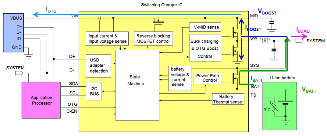
Figure 13
Programmable boost converter current limit allows the OTG output to be made compatible with USB port capability.
Some chargers allow disabling the reverse blocking MOSFET, and the boosted voltage on the MID pin can be used as separate 5V output like in power banks.
Charging with higher input voltage
At 5V input voltage, a high battery charge current quickly results in high input current as well, since the Li-Ion battery voltage is not much lower than 5V. Adapter current limit and cable / connector current limitations will become the limiting factor for maximum charge current. (For example, the micro USB connector max current rating is around 1.8A). Modern switching chargers have higher operation input voltage ratings, which makes it possible to run them from supplies higher than 5V, for example 9V or 12V. Since the input current of step-down switching chargers is defined by: 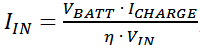 , a higher input voltage will reduce input current. It should be noted that higher input voltage also will increase converter switching losses, thereby reducing conversion efficiency. This can be compensated somewhat by reducing switching frequency, at the expense of larger filter components.
Variable VBUS voltage charging systems that make use of the USB port will default start in 5V input condition, to avoid damage to standard 5V-only systems. After connection, a communication has to take place between charger and adapter to make sure the USB BUS voltage can be increased without damaging the charger circuit. Several companies have developed special communication methods to accomplish this:
Qualcomm has developed QuickCharge™ which uses the D+ and D- lines to communicate with the adapter.
MediaTek has developed MTK Pump Express™, where the charger uses input current modulation to communicate with the adapter.
Both systems will increase the adapter voltage based on a voltage request from the charger.
Devices which use the new USB-C port are able to use the standardized USB-C Power Delivery protocol for communication between charger and adapter and set the BUS voltage between 5V and 20V with currents up to 5A.
Richtek has a wide portfolio of single-cell Li-Ion chargers divided in Linear Chargers, Switching Chargers and Wireless Chargers. In this section we describe 3 types of switching chargers with different capabilities: RT9458, RT9460 and RT9466. The basic differences between the 3 devices are listed in below comparison tables.
Comparison tables
Basic functionality overview
|
Function
|
RT9458
|
RT9460
|
RT9466
|
|
Charger power stage
|
1.5MHz synchronous
|
0.75/1.5MHz synchronous
|
0.75/1.5MHz synchronous
|
|
Battery charging
|
1.55A max single cell
|
3A max single cell
|
5A max single cell
|
|
Adapter voltage
|
5V
|
5V~12V
|
5V~14V
|
|
Dynamic Power Path
|
No
|
Yes, with ext MOS option
|
Yes, internal MOS
|
|
OTG On-The-Go boost function
|
Yes, 1A
|
Yes, 1A
|
Yes, 2.4A
|
|
NTC sense function
|
No
|
Yes, JEITA with CC adj.
|
Yes, JEITA with CC&CV adj.
|
|
USB Charging Detection
|
No
|
Yes, BC1.2
|
No
|
|
Input current limit setting
|
I2C
|
I2C
|
I2C and external resistor
|
|
Shipping mode
|
No
|
No
|
Yes
|
|
Factory mode
|
No
|
No
|
Yes
|
|
IR drop compensation
|
No
|
No
|
Yes
|
|
Status outputs
|
No
|
Yes, charge Status
|
Yes CH-STAT and VBUS-PG
|
|
Actual charge current reporting
|
No
|
No
|
Yes
|
|
Spread Spectrum EMI reduction
|
No
|
Yes
|
No
|
|
MTK Pump Express support
|
No
|
No
|
Yes, MTK PE1.0 & 2.0
|
|
Stand-alone operation
|
No, needs I2C
|
Yes, see default settings
|
Yes, ILIM resistor & default
|
|
Package
|
WL-CSP-20B2.1x1.87mm
|
WL-CSP-25B2.52x2.52mm
|
WQFN-24L 4x4
|
Charging parameters details:
|
Parameter
|
RT9458
|
RT9460
|
RT9466
|
|
Input voltage max rating
|
20V
|
28V
|
22V
|
|
Input voltage operation range
|
4.3V ~ 6V
|
4.3~12V
|
4.0~14V
|
|
Charge current
|
0.5~1.55A (150mA step) (default 0.5A)
|
1.25~3.125A (125mA step) (default 1.25A)
|
0.1~5A (100mA step)
(default 2A)
|
|
Charge Voltage
|
3.5~4.45 (20mV step, 1%)
(Default 4.2V)
|
3.5~4.62 (20mV step, 1%)
(Default 4.0V)
|
3.9~4.71 (10mV step, 1%)
(Default 4.2V)
|
|
Input current control (AICR)
|
0.1/0.5/0.7A/disable
(default 0.5A)
|
0.1~3A/disable (0.1A step)
(default 0.5A)
|
0.1~3.25A / disable 0.1A step, default via R-ILIM)
|
|
Input voltage control (MIVR)
|
4.1~4.7/disable (0.1V step) (default 4.5V)
|
4.0~15.5/dis (0.25V step) (default 4.0V)
|
3.9~13.4/dis (0.1V step)
(default 4.4V)
|
|
Pre-charge voltage
|
2V~3V (0.2V step)
(default 2.4V)
|
2V~3V (0.2V step)
(default 2.4V)
|
2V~3.5V (0.1V step)
(default 3V)
|
|
Pre-charge current
|
20~60mA (20mA step)
(default 60mA)
|
100~850mA (50mA step)
(default 250mA)
|
100~850mA (50mA step)
(default 150mA)
|
|
End of Charge current
|
50~400mA (50mA step)
(default 150mA)
|
100~450mA (50mA step)
(default 200mA)
|
100~850mA (50mA step)
(default 250mA)
|
|
IR compensation
|
No
|
No
|
0~175mΩ (25mΩ step)
0~224mV clamp 32mV step
|
OTG On-The-Go Boost parameters:
|
Parameter
|
RT9458
|
RT9460
|
RT9466
|
|
OTG maximum output current
|
1A
|
0.5A/1A
(default 0.5A)
|
0.5~2.4A (300mA step)
(default 0.5A)
|
|
OTG regulation Voltage
|
4.425~5.6V (25mV step, 1%)
(Default 5.325V)
|
4.425~5.825V (25mV step, 1%) (Default 5.05V)
|
4.425~5.825V (25mV step, 1%) (Default 5.05V)
|
|
OTG minimum battery voltage
|
2.9V start/ 2.5V operation
|
2.9V start/ 2.5V operation
|
2.3V~3.8V falling 0.4V hys, 0.1V step (2.8V default)
|
Protection functions:
|
Parameter
|
RT9458
|
RT9460
|
RT9466
|
|
Input overvoltage protection
|
Yes, 6.7V typical
|
Yes, 16V typical
|
Yes, 14.5V typical
|
|
Input bad adapter protection
|
No
|
Yes
|
Yes, VBUS <3.8V @ 50mA
|
|
Battery absence protection
|
Yes
|
Yes
|
Yes
|
|
Battery OVP
|
Yes, > 117 ± 6%
|
Yes, > 117 ± 6%
|
Yes, 108 ± 2%
|
|
Thermal regulation
|
Yes, I-charge reduce when temperature > 120oC
|
Yes, I-charge reduce when temperature > 120oC
|
Yes, I-charge reduce temp >60/80/100/(120oC default)
|
RT9458 is a basic switching charger, mainly intended for applications to replace linear chargers for better system efficiency and more optimal charging with low input current adapters. It is capable of delivering 1.5A charge currents, and can be used for small and medium capacity Li-Ion batteries up to around 1.8Ah.
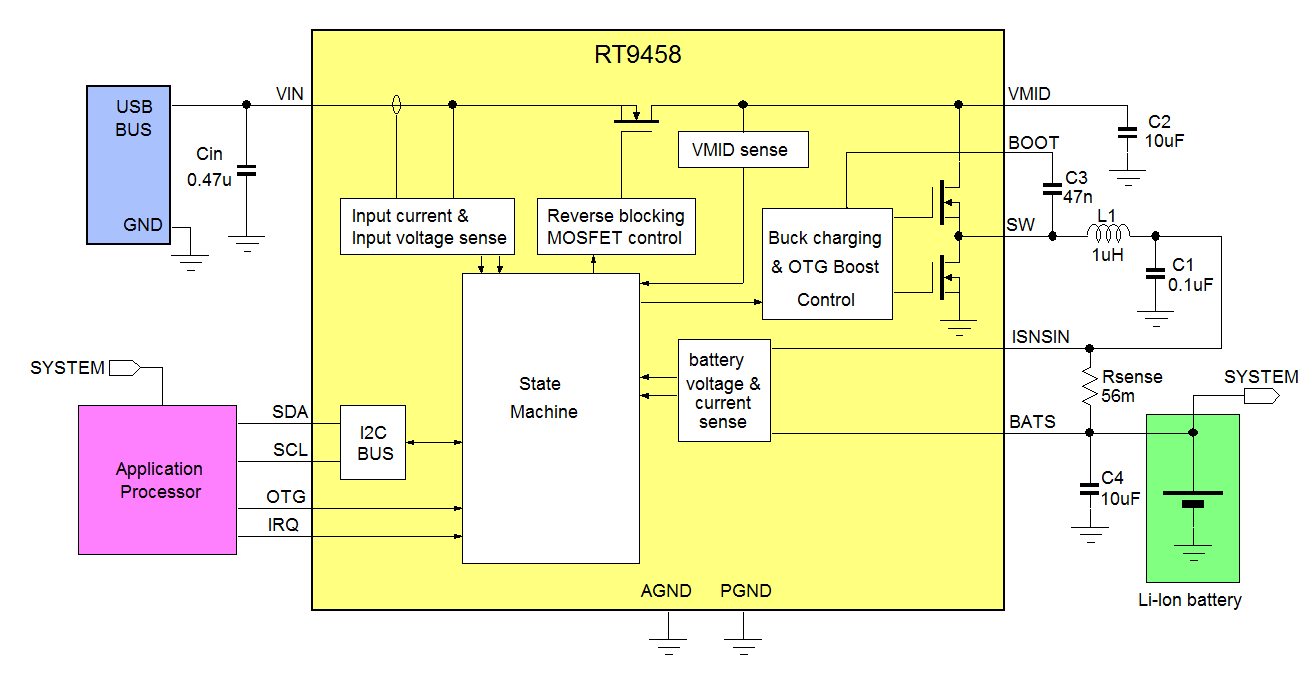
Figure 14
Figure 14 shows the standard application. RT9458 uses an external resistor for sensing the battery charging current. This charger does not have power path control, so the battery voltage directly supplies the system.
RT9458 needs I2C control for normal charging because it uses a timer watchdog that needs to be reset regularly. It therefore cannot be used as stand-alone charger.
Figure 15 shows the advantage of the RT9458 switching charger over a linear charger in an application with 500mA USB input current limit: In linear chargers, the maximum charge current equals the input current which is limited to 500mA in this case. For a switching charger, the max charge current will higher than the 500mA input current limit, especially at lower battery voltage. This will result in shorter charge time and less heat losses in the charger IC.
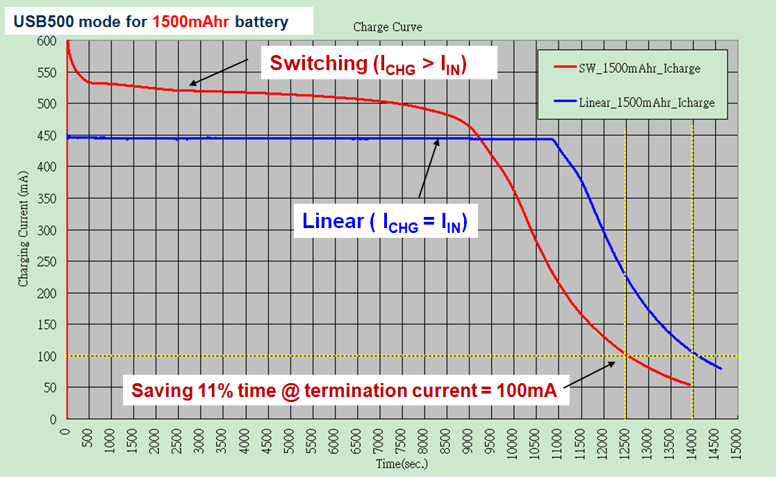
Figure 15
Design resources
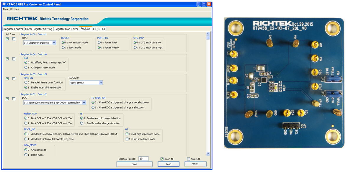
Figure 16
RT9458 evaluation kit comes with an evaluation board which contains all components and options to test all functions of the device. Furthermore an extensive GUI is provided for reading and writing all registers via I2C using the Richtek Wrenboard utility. See figure 16.
RT9460 is a more advanced switching charger, with Adapter Detection, up to 3A charge current, Dynamic Power Path control, battery temperature sensing and a wide input voltage range of 4.3 – 12V. It can be used for portable devices with larger capacity battery packs like 2.5~2.8Ah. The Adapter Detection makes it possible to detect BC1.2 and several brand-specific adapter types, which allows selection of the optimal input current limit for the specific input source, to achieve the maximum charge current without overloading the input source.
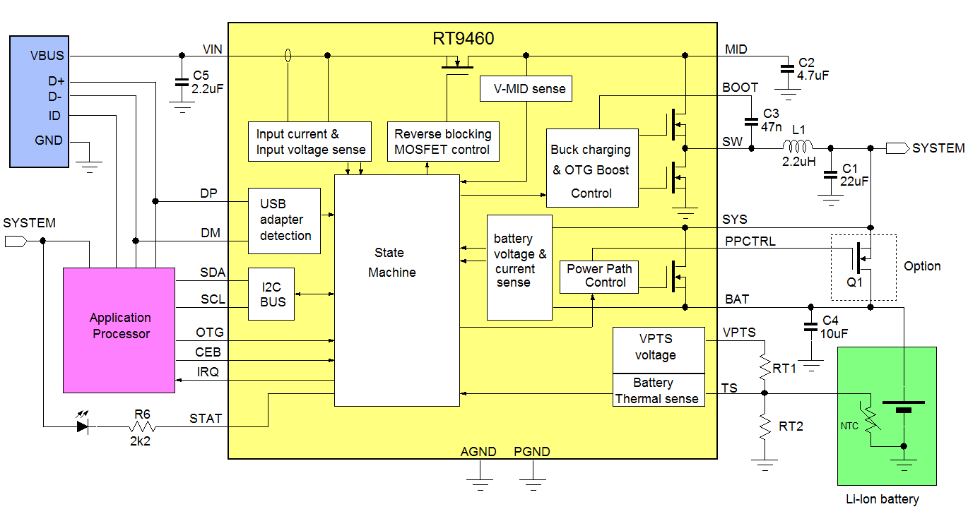
Figure 17
Figure 17 shows the typical application circuit. When input voltage is applied via the USB port, RT9460 will go through a sequence of Adapter Detection, checking the D+/D- lines for various voltage levels, connections and handshakes, to determine the Adapter Port current capability. The result can be read from internal registers.
In charging mode, the switching buck stage produces an output voltage for SYSTEM and a charge current to the battery. The battery current is sensed by the internal power path MOSFET. The external MOSFET Q1 is off. When the adapter is removed, the battery provides the system voltage via the power path control MOSFET. The (optional) external MOSFET Q1 can be switched on to reduce the voltage drop between BAT and SYS.
In OTG mode, the switching stage works as BOOST and provides a regulated OTG voltage on the MID pin, which is transferred to VIN via the reverse blocking MOSFET. Two different OTG current (0.5A & 1A) limits can be set. Battery temperature can be sensed via the NTC and 5 JEITA temperature ranges are defined. Charge current can be changed in cool and warm temperature range.
RT9460 can be operated in stand-alone charger conditions, but without I2C control, the charge conditions are limited to the following default values: Charging current 1.25A, battery regulation voltage 4.0V. Input current limit based on OTG pin setting: OTG low: AICR = 500mA and OTG high: AICR = 1A. OTG boost must be enabled via I2C.
The wide input voltage range makes it possible to run RT9460 from higher input sources like 9V or 12V. It is possible to implement the MTK Pump Express™ function by modulating the input current control register via I2C via the application processor, to request higher VBUS voltage from a Pump Express compatible adapter. RT9460 can also be used in combination with USB-C PD controllers, where VBUS voltage can be increased via Power Delivery protocol.
Design resources
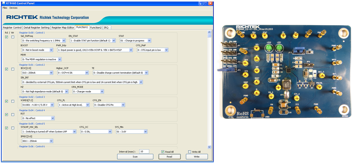
Figure 18
RT9460 evaluation kit comes with an evaluation board which contains all components and options to test all functions of the device. Furthermore an extensive GUI is provided for reading and writing all registers via I2C using the Richtek Wrenboard utility. See figure 18
RT9466 is a powerful switching charger with 4-14V input range and battery charge current up to 5A, designed to charge larger size Li-Ion packs used in high-end smart-phone and tablet PCs (battery capacity ranging from 3 - 4Ah). Charging at these high currents requires careful battery condition monitoring. RT9466 features accurate battery voltage and charge current measuring and reporting, programmable IR sensing, accurate battery overvoltage protection, programmable thermal charge reduction, and extremely low Rdson power path and switching MOSFETs. The typical application circuit is shown in figure 19.
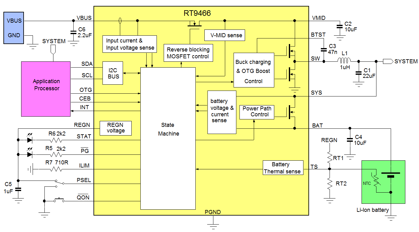
Figure 19
RT9466 has a number of pins that can be used to set charging conditions without using I2C:
PSEL pin is the Power source select pin: PSEL=high will set input current at 500mA for standard USB port use. PSEL=low will set the input current limit at 3.25A for power adapter input application.
A resistor R-ILIM connected to the ILIM pin will program the maximum input current limit based on 355AΩ/R-ILIM. In default start-up condition, the input current is limited by the smallest value of either PSEL or ILIM.
Charging condition indication can be signaled via the STAT pin, and PG pin can be used to detect VBUS under voltage or overvoltage conditions.
RT9466 power path function also includes a shipping mode, where the system is disconnected from the battery, thereby minimizing battery leakage. The QON pin can be used to exit shipping mode.
Battery temperature can be sensed via the NTC and 5 JEITA temperature ranges are defined. Both charge current and charge regulation voltage can be changed in cool and warm temperature range.
RT9466 has a powerful OTG function with max current capability of 2.4A. OTG regulation voltage and current limit are programmable via I2C.
RT9466 can be operated in stand-alone charger conditions, but without I2C control, the charge conditions are limited to the following default values: Charging current 2A, battery regulation voltage 4.2V. Input current limit based on PSEL pin setting and ILIM resistor. Charge current termination is default disabled, which means that RT9466 will trickle charge in stand-alone mode. OTG boost function must be enabled via I2C.
RT9466 IR compensation function
|
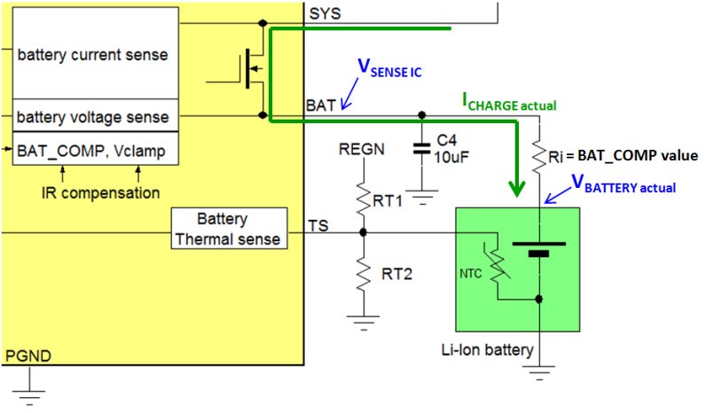
Figure 20
|
High charge current will lead to errors in correct battery voltage reading by the IC due to voltage drop across PCB traces and the battery internal resistance. This error can be compensated by activating the IR compensation in RT9466 via the BAT_COMP register and VCLAMP register. BAT_COMP register can be set from 0Ω to 175mΩ in 25mΩ increments. The RT9466 will add a voltage offset to the sensed battery voltage which equals ICHARGE actual * BAT_COMP. The maximum offset can be limited by setting the VCLAMP register.
The designer should make sure that the BAT_COMP value is chosen conservatively to ensure overcharging of the battery will not occur. Setting a correct BAT_COMP will extend the fast-charging CC mode, thereby reducing total charge time. This is illustrated in an actual measurement of a 2A charging application with a total resistance of PCB trace and battery internal resistance of 50mΩ. By setting BAT_COMP at 50mΩ, the total charging time can be reduced by 18 minutes. See figure 21.
|
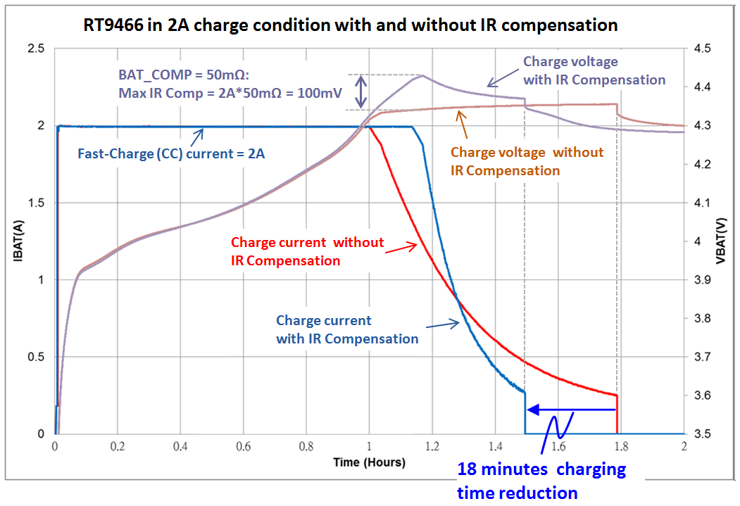
Figure 21
Mediatek Pump Express function
RT9466 includes all necessary hardware and logic to implement MTK Pump Express™ (PE+) 1.0 and 2.0. When enabling the PE+ function, the charger will generate an input load current pattern according the PE+ standard.
When a PE+ compliant adapter is connected, it will recognize this load current modulation, and adjust the output voltage to various levels based on the PE+ command received. The system flow is shown in figure 22.
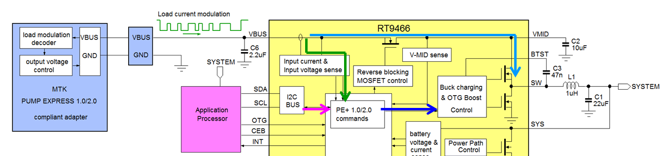
Figure 22
PE+ 1.0 allows VBUS voltage increase and decrease between 5V/7V/9V/12V. PE+ 2.0 allows VBUS voltage adjustment from 5.5V ~ 20V in 0.5V steps. It also allows adapter health checking and enable/disable adapter cable drop compensation. The higher bus voltage will lower the input current, and this will allow higher charging currents without exceeding adapter current limit or cable/connector current limitations.
Figure 23 shows PE+2.0 load current communication method, which consists of a 150msec start period, 5 bits, 190msec end period and watchdog timeout period. The 5 bits logic high/low state is defined by the load current high/low level pulse width. The load current high/low state must be higher/lower than the H and L detection level thresholds.
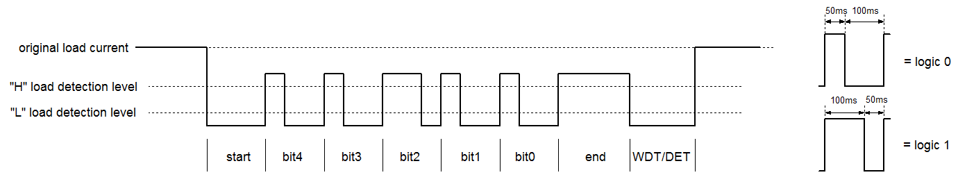
Figure 23
Figure 24 shows a measurement of RT9466 in a PE+ 2.0 compatible adapter application where a 12.0V VBUS voltage request was executed. Initially, the BUS voltage is 5V, and the 2A battery charge current results in an input current of about 1.8A. When the 12V VBUS request is executed, the RT9466 will modulate the input current between maximum and minimum current based on the PE+ 2.0 protocol. (In this case the pattern is 01101, which corresponds with a 12V request). Due to dynamic load variation, the BUS voltage will also slightly vary. After the command is executed, the PE+ 2.0 compatible adapter will change its output voltage to 12V. The charger will operate at its original 2A charge current again, but the input current is reduced considerably due to the higher VBUS voltage. Charge current can now be increased without exceeding the input USB cable and connector current ratings.
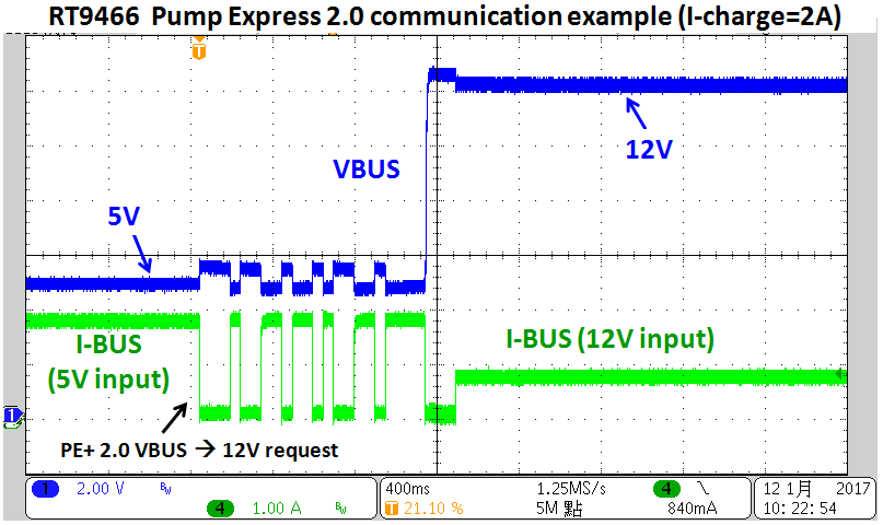
Figure 24
Master-slave charging
Although RT9466 can provide charge currents up to 5A, it cannot do so continuously due to thermal limitations in small mobile environments. Mobile applications that require charge currents higher than 3A normally use master-slave charging: In these applications a second switching charger is added in parallel with RT9466 which can be activated when high charge currents like 4.5 ~ 5A are needed, for a longer period. The slave charger does not need the full functionality of a switching charger, and consists of a buck switching stage, battery voltage sensing and I2C bus. Figure 25 below shows a master-slave charging application using RT9466 and RT9465 simple charger as slave.
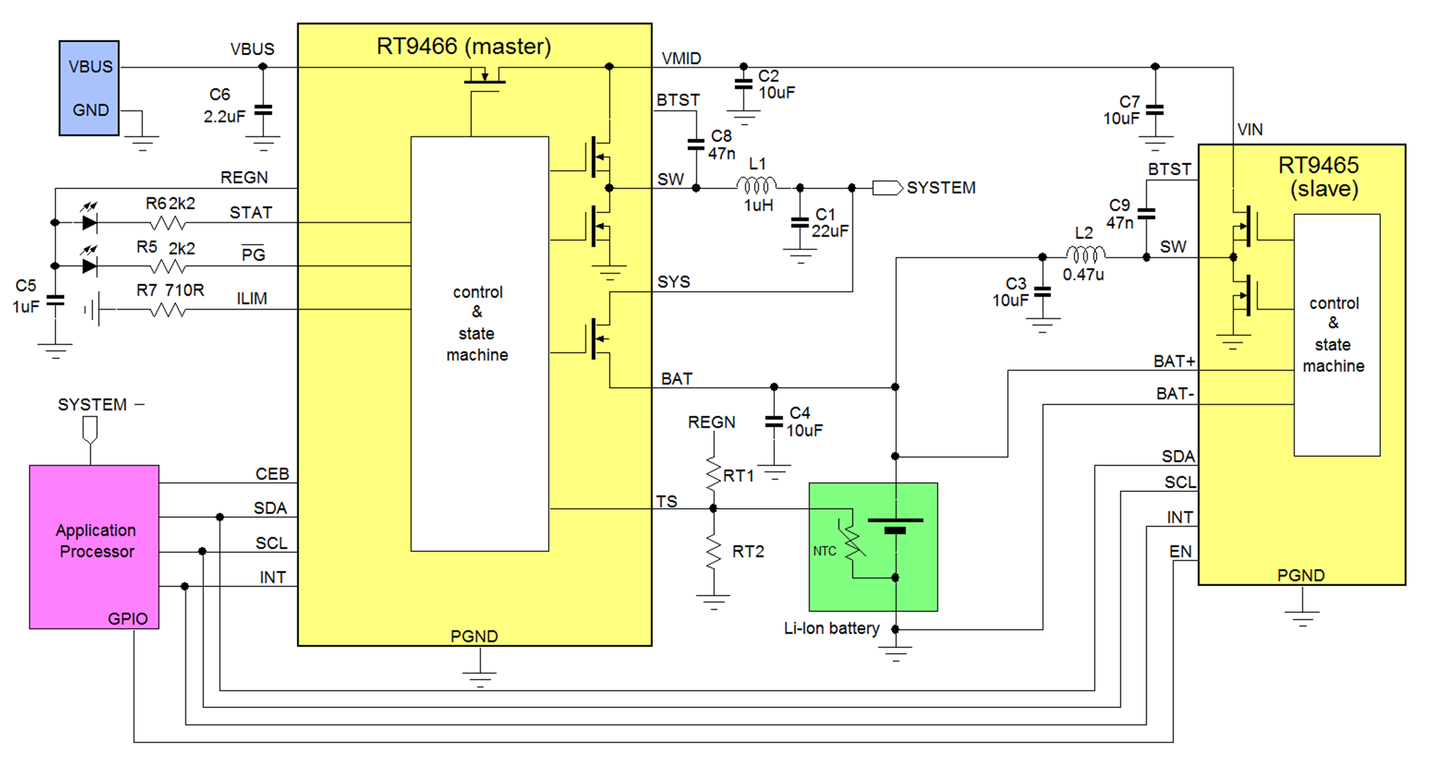
Figure 25
In Master-Slave operation, the master charger is used to detect the battery charging conditions, like pre-charge, CC mode, CV mode and end of charge termination. When the master charger is in CC mode, the AP will set the slave in constant current mode to increase the fast-charging current. During this mode the junction temperature of the two charging devices is monitored, and charge current adjustments are made to keep the temperatures within certain limits. When the master enters the CV mode, the current of the slave is gradually lowered by the AP, and at a certain point it is completely switched off, allowing the master to finish the charging cycle. Figure 26 shows an example charging cycle using master-slave operation with IR compensation. In this example, a 3Ah battery can be fully charged within one hour.
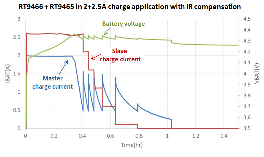
Figure 26
USB-C Power Delivery application
Mobile devices that support the USB-C port with Power Delivery function (PD) can make use of the PD communication between downstream port and upstream port to set the VBUS voltage to a higher value, between 5V and 20V and currents up to 5A. USB-C with dual role function also allows the mobile device to act as power source to deliver current to connected devices. Figure 27 shows an example application where USB-C PD controller RT1711H communicates with connected devices over the USB-C CC lines, and configures the VBUS based on operating conditions set by the application processor and RT9466 charger IC.
In provider role, RT1711 can communicate the RT9466 OTG capabilities to a consumer device and activate RT9466 OTG function via the AP to power VBUS from the battery via OTG boost.
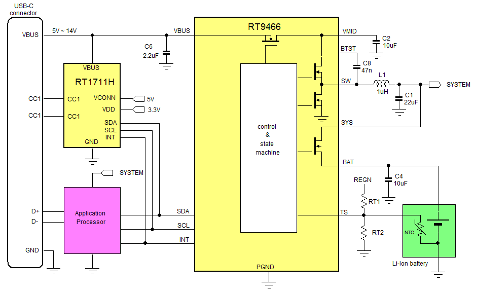
Figure 27
Design resources
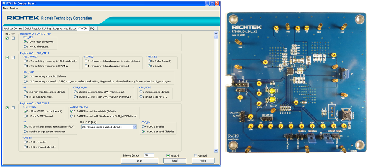
Figure 28
RT9466 evaluation kit comes with an evaluation board which contains all components and options to test all functions of the device. Furthermore an extensive GUI is provided for reading and writing all registers via I2C using the Richtek Wrenboard utility. See figure 28
6.Summary
Fast charging of portable devices with larger capacity Li-Ion batteries requires careful considerations of input source capability, battery characteristics, charger capability and thermal effects. Richtek has several switching chargers with many integrated functionality to make optimal use of connected hardware and software to safely charge a wide range of battery packs. Please visit the Richtek website for datasheets and design tools, and contact your nearest Richtek sales representative for samples or evaluation boards.