1.Introduction
SOT-23 packages are popular due to their small footprint and low cost, while the 6-pin and 8-pin versions still allow to them to be used in various applications like LDOs and switching regulators.
One of the drawbacks of SOT-23 package is their limited power dissipation capability, because these packages have no thermal pad.
Standard wire bond SOT-23-6 package thermal resistance in a JEDEC thermal reference board shows θJA values (Thermal resistance from junction to ambient) of around 220 ~ 250oC/W, which means that in applications where ambient temperatures are around 55oC, an IC dissipation of 0.3W already reaches the max recommended junction temperature of 125oC.
In actual PCB layout, there are some ways to increase the power dissipation capabilities, by increasing the width of the traces connected to the pins, but the effectiveness of these measures depends a lot on the inner structure of the SOT-23 package.
Traditional wire bond packages behave quite different thermally when compared to Flip-Chip-On-Lead (FCOL) packages. In order to make the best PCB layout, it is important to know a bit more about the internal structure of the two package types.
2.Wire-Bond SOT-23-6 package structure
Figure 1 below shows the basic structure of a wire-bond SOT-23-6 package.
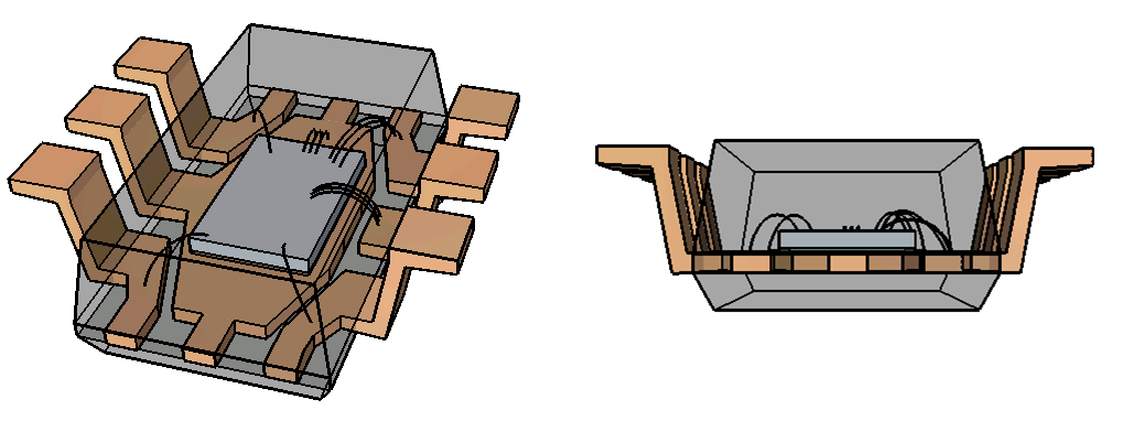
Figure 1
The silicon die is glued to the center ground lead, and the die electrical connections are wired to the lead frame pins via bonding wires, which are typically 25-38um gold or copper wires.
These thin wires add resistance, inductance and stray capacitance to critical circuit nodes, which reduces the performance of high frequency switching converters. Especially in higher current buck converters, the bonding wires can play a significant role in the total power loss of the device.
The thin bonding wires are also poor heat conductors, so most of the potential heat transfer of the pins is lost. Heat transfer is mostly from the back side of the die through adhesive to the center ground pin, causing a hot spot on the center pin.
Figure 2 shows a thermal image simulation of a wire-bond SOT-23-6 package in a buck converter application.
The device power dissipation was set at 0.5W.
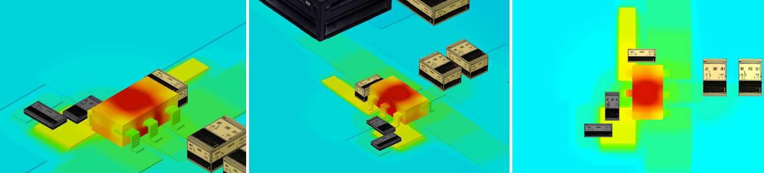
Figure 2
It can be clearly seen that the temperature of the center pin is much higher than the adjacent pins. This single pin is limited in conducting all the heat from the die to the PCB, and a hot spot forms around the device center pin.
3.FCOL SOT-23-6 package structure
Figure 3 below shows the inner construction of a Flip-Chip-On-Lead SOT-23-6 package.
(The die is made transparent for clarity)
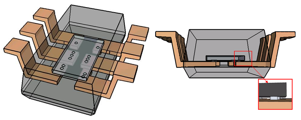
Figure 3
The top side of silicon die is mounted via pillar bonding to the lead frame providing both the thermal and electrical connections directly from silicon die to the lead frame.
The short interconnect length of pillar bonding delivers significantly less resistance, inductance and stay capacitance, which minimizing I2R and switching losses while reducing waste heat.
All pins are now acting as small heat sinks, and can be used for efficient cooling, so there is more heat transfer from package to PCB, resulting in lower die temperature. Figure 4 shows a thermal simulation of the FCOL package with the same 0.5W device power dissipation.
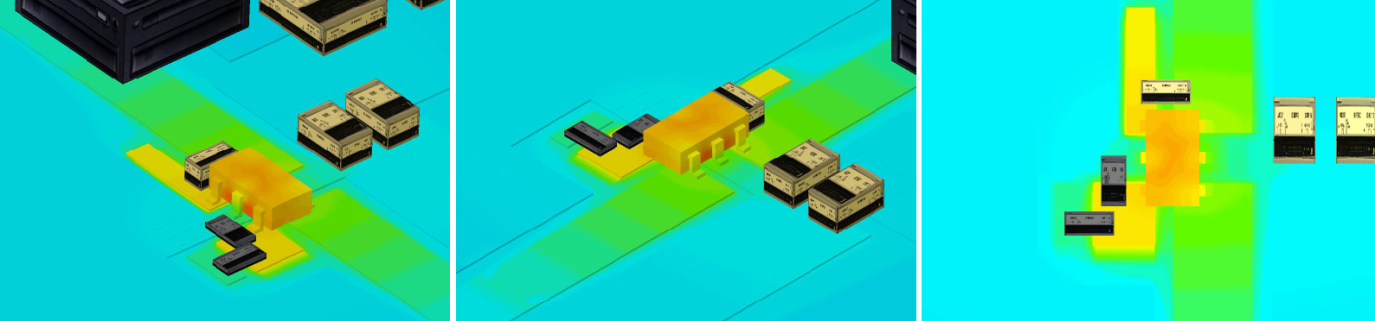
Figure 4
The thermal simulation clearly shows the more even heat conduction of the FCOL package to all pins, and there is no clear hot spot around the center pin.
4.Tips for SOT-23 PCB layout
It is clear that wire bond and FCOL SOT-23 packages have some clear differences in their thermal conduction properties to the device pins. The PCB designer can use this knowledge to optimize the PCB layout for each package.
Figure 6 shows an example layout using RT7295CGJ6F, which is a 3.5A Buck converter in FCOL SOT-23 based on Richtek’s ACOT® topology. (The “F” suffix stands for FCOL). The simple schematic is shown in figure 5.
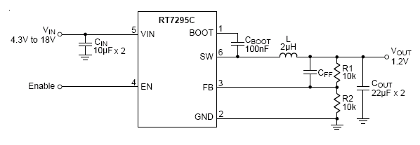
Figure 5
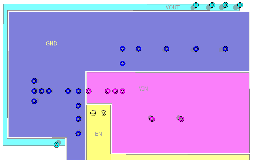
The basic setup is shown below. It makes use of a 4-layer board. Standard vias are used to make connections to the inner layers and bottom layer.
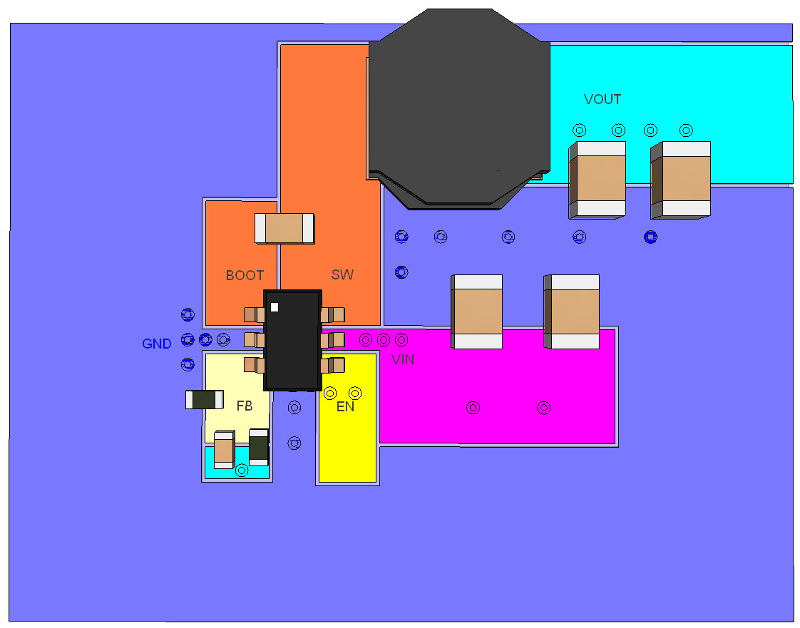
Figure 6
In the layout of figure 6, each pin has extra copper. For the Boot and SW pins, large copper planes may cause extra radiation, so a compromise must be made. The FB pin is sensitive for noise pickup, so cannot have a large copper area either. The GND and VIN pins are connected with several vias to inner layer copper planes. The enable pin can also have some extra copper and is connected to bottom layer.
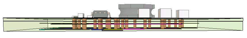
Figure 7
The PCB cross section shows the vias and inner layers on scale. Vias are quite effective in conducting heat from top layer to other layers. Extra vias can be added for better heat conduction.
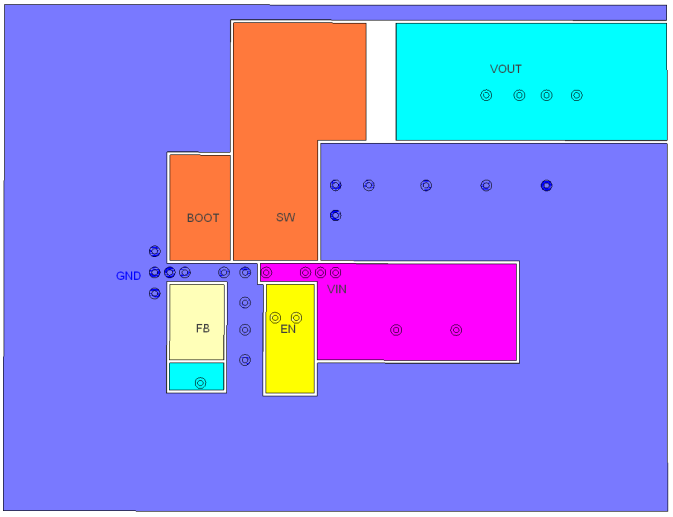
Below table shows the layout of the different layers.
|
|
|
|
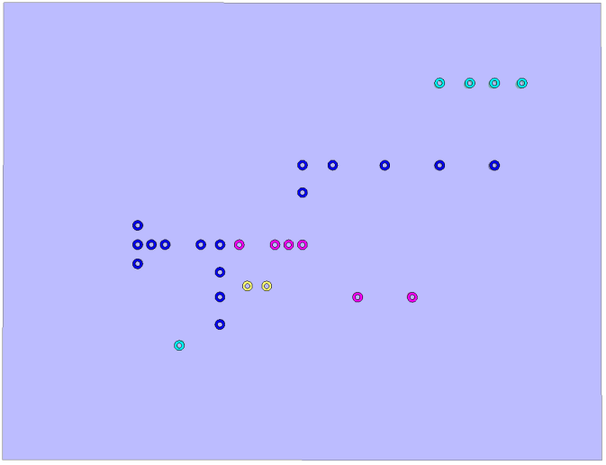
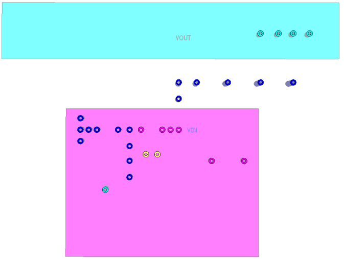
Top layer: copper planes at SW, BOOT (orange), Enable (yellow), FB (beige), VIN (purple), GND (blue).
It is important to place vias close to the IC pins.
|
Second layer is solid ground plane. Extra GND vias (blue) close to IC GND pin.
|
|
|
|
|
Third layer is supply layer. Extra vias (purple) from IC VIN to purple Vin layer. Copper planes for GND and EN signal could also be added here.
|
Bottom layer has yellow vias to Enable plane, purple vias to VIN plane and blue vias to GND plane.
|
The above layout is just for reference. In some PCB designs, the top and bottom layer may not have so much space. In those cases, IC pins can be connected with vias to copper planes in the inner layers. It is important to realize that in FCOL packages all IC pins are potential heat conductors, and good thermal connection to PCB copper planes can enhance the thermal cooling effect.
5.Thermal measurements
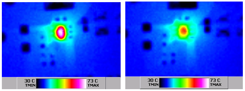
Figure 8
Figure 8 shows two thermal scans: Left is a standard wire-bond SOT-23-6 package, while the right scan shows an FCOL SOT-23-6. Both ICs were mounted on a Richtek evaluation board with the same device power dissipation of around 0.7W. The layout was optimized for good thermal performance based on guidelines mentioned in Chapter 4. The wire bond SOT-23-6 clearly shows a large hotspot, and the scan also shows that the pins on the left side of the package are hotter than the pins on the right side. This is because the GND pin is located on the left side. The FCOL package hotspot is around 20 ~ 30 degrees cooler than the wire bond, and shows even heat conduction from all pins.
Based on above results, the thermal resistance from junction to ambient of an FCOL SOT-23-6 package in a highly optimized layout can go as low as 55oC/W . In layouts were there is less space available, the cooling properties may be a bit less, but values of 70~80oC/W are definitely achievable. This makes it possible to dissipate around 0.85W under 60oC ambient conditions.
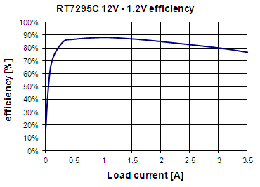
Figure 9
Figure 9 shows the efficiency graph of RT7295C for 12V to 1.2V application.
The IC losses at 3.1A load are around 0.85W.
This means that when RT7295C is applied in a thermally enhanced layout, the device can definitely deliver 3A load currents without overheating.
6.Summary
FCOL packages have some electrical and thermal advantages. In FCOL packages each pin has a good thermal connection to the silicon die. The PCB layout can be optimized to let each pin conduct more heat from die to PCB, which can lower the overall thermal resistance from Junction to Ambient. This allows more power to be dissipated in the FCOL package when compared to same package with wire bond connections.