Richtek 42V/60V Industrial and Automotive Buck Converters
Abstract
The RTQ2960/61/62/63/65 and RTQ6360/61/62/63/65 are flexible buck converter families for wide input and output voltage range applications. They can be used with input voltages from 4.5V up to 60V and the output can be adjusted from 0.8V up to VIN. The RTQ2960/61/62/63/65 and RTQ2940/41/42/43/49/49A/45/45A are Automotive Grade 1 buck converters that are suitable to be used in 12V car battery systems (42V rating) and 24V car battery systems (60V rating) and include the spread-spectrum feature. The RTQ6360/61/62/63/65 and RTQ6340/41/42/43/45 are Industrial Grade buck converters that are suitable to be used in applications requiring steady fixed frequency operation and industrial temperature range.
The buck converter ranges include parts that can deliver currents from 0.5A up to 5A output currents. This application note explains the design criteria and describes two wide input voltage step-down designs: A low power 3.3V/0.5A output using RTQ6360GQW and a high power 24V/3A output using RTQ6363GQW. External components are calculated using the RTQ29xx and RTQ63xx Excel based design tools, and results are verified with actual measurement results.
1.
Introduction
The RTQ2960/61/62/63/65, RTQ6360/61/62/63/65, RTQ2940/41/42/43/49/49A/45/45A and RTQ6340/41/42/43/45 are flexible asynchronous buck converter families for wide input and output voltage range applications. The parts can be used with input voltages from 4.5V up to 42V for RTQ2940/41/42/43/49/49A/45/45A and RTQ6340/41/42/43/45 and 4.5V to 60V for the RTQ2960/61/62/63/65 and RTQ6360/61/62/63/65 parts, and the output can be adjusted from 0.8V up to VIN, delivering up to 5A output currents, and use peak current mode topology with external compensation for optimal flexibility.
The RTQ2960/61/62/63/65 and RTQ2940/41/42/43/49/49A/45/45A are Automotive Grade 1 buck converters that include the spread-spectrum feature. The RTQ6360/61/62/63/65 and RTQ6340/41/42/43/45 are Industrial Grade buck converters without spread spectrum feature. All the IC families support enhanced light load efficiency and low dropout mode operation approaching 100% duty-cycle.
|
Part number
|
Vin range
|
Current rating
|
Programmable Frequency range
|
RDSON
|
TON_MIN
|
External compensation
|
External soft-start
|
Power good
|
Spread Spectrum/AEC-Q100
|
Package
|
|
RTQ6360GSP
|
4.5 ~ 60V
|
0.5A
|
0.1 ~ 2.5MHz
|
170mΩ
|
100ns
|
Yes
|
No
|
No
|
No
|
PSOP-8
|
|
RTQ6360GQW
|
4.5 ~ 60V
|
0.5A
|
0.1 ~ 2.5MHz
|
170mΩ
|
100ns
|
Yes
|
Yes
|
Yes
|
No
|
DFN10L 3x3
|
|
RTQ6361GSP
|
4.5 ~ 60V
|
1.5A
|
0.1 ~ 2.5MHz
|
160mΩ
|
100ns
|
Yes
|
No
|
No
|
No
|
PSOP-8
|
|
RTQ6361GQW
|
4.5 ~ 60V
|
1.5A
|
0.1 ~ 2.5MHz
|
160mΩ
|
100ns
|
Yes
|
Yes
|
Yes
|
No
|
DFN10L 3x3
|
|
RTQ6362GSP
|
4.5 ~ 60V
|
2.5A
|
0.1 ~ 2.5MHz
|
150mΩ
|
100ns
|
Yes
|
No
|
No
|
No
|
PSOP-8
|
|
RTQ6362GQW
|
4.5 ~ 60V
|
2.5A
|
0.1 ~ 2.5MHz
|
150mΩ
|
100ns
|
Yes
|
Yes
|
Yes
|
No
|
DFN10L 3x3
|
|
RTQ6363GSP
|
4.5 ~ 60V
|
3.5A
|
0.1 ~ 2.5MHz
|
80mΩ
|
120ns
|
Yes
|
No
|
No
|
No
|
PSOP-8
|
|
RTQ6363GQW
|
4.5 ~ 60V
|
3.5A
|
0.1 ~ 2.5MHz
|
80mΩ
|
120ns
|
Yes
|
Yes
|
Yes
|
No
|
DFN10L 4x4
|
|
RTQ6365GSP
|
4.5 ~ 60V
|
5A
|
0.1 ~ 2.5MHz
|
70mΩ
|
120ns
|
Yes
|
No
|
No
|
No
|
PSOP-8
|
|
RTQ6365GQW
|
4.5 ~ 60V
|
5A
|
0.1 ~ 2.5MHz
|
70mΩ
|
120ns
|
Yes
|
Yes
|
Yes
|
No
|
DFN10L 4x4
|
|
|
|
RTQ2960GSP
|
4.5 ~ 60V
|
0.5A
|
0.1 ~ 2.5MHz
|
170mΩ
|
100ns
|
Yes
|
No
|
No
|
Yes
|
PSOP-8
|
|
RTQ2960GQW
|
4.5 ~ 60V
|
0.5A
|
0.1 ~ 2.5MHz
|
170mΩ
|
100ns
|
Yes
|
Yes
|
Yes
|
Yes
|
DFN10L 3x3
|
|
RTQ2961GSP
|
4.5 ~ 60V
|
1.5A
|
0.1 ~ 2.5MHz
|
160mΩ
|
100ns
|
Yes
|
No
|
No
|
Yes
|
PSOP-8
|
|
RTQ2961GQW
|
4.5 ~ 60V
|
1.5A
|
0.1 ~ 2.5MHz
|
160mΩ
|
100ns
|
Yes
|
Yes
|
Yes
|
Yes
|
DFN10L 3x3
|
|
RTQ2962GSP
|
4.5 ~ 60V
|
2.5A
|
0.1 ~ 2.5MHz
|
150mΩ
|
100ns
|
Yes
|
No
|
No
|
Yes
|
PSOP-8
|
|
RTQ2962GQW
|
4.5 ~ 60V
|
2.5A
|
0.1 ~ 2.5MHz
|
150mΩ
|
100ns
|
Yes
|
Yes
|
Yes
|
Yes
|
DFN10L 3x3
|
|
RTQ2963GSP
|
4.5 ~ 60V
|
3.5A
|
0.1 ~ 2.5MHz
|
80mΩ
|
120ns
|
Yes
|
No
|
No
|
Yes
|
PSOP-8
|
|
RTQ2963GQW
|
4.5 ~ 60V
|
3.5A
|
0.1 ~ 2.5MHz
|
80mΩ
|
120ns
|
Yes
|
Yes
|
Yes
|
Yes
|
DFN10L 4x4
|
|
RTQ2965GSP
|
4.5 ~ 60V
|
5A
|
0.1 ~ 2.5MHz
|
70mΩ
|
120ns
|
Yes
|
No
|
No
|
Yes
|
PSOP-8
|
|
RTQ2965GQW
|
4.5 ~ 60V
|
5A
|
0.1 ~ 2.5MHz
|
70mΩ
|
120ns
|
Yes
|
Yes
|
Yes
|
Yes
|
DFN10L 4x4
|
|
|
|
RTQ6340GSP
|
4.5 ~ 42V
|
0.5A
|
0.1 ~ 2.5MHz
|
170mΩ
|
100ns
|
Yes
|
No
|
No
|
No
|
PSOP-8
|
|
RTQ6340GQW
|
4.5 ~ 42V
|
0.5A
|
0.1 ~ 2.5MHz
|
170mΩ
|
100ns
|
Yes
|
Yes
|
Yes
|
No
|
DFN10L 3x3
|
|
RTQ6341GSP
|
4.5 ~ 42V
|
1.5A
|
0.1 ~ 2.5MHz
|
160mΩ
|
100ns
|
Yes
|
No
|
No
|
No
|
PSOP-8
|
|
RTQ6341GQW
|
4.5 ~ 42V
|
1.5A
|
0.1 ~ 2.5MHz
|
160mΩ
|
100ns
|
Yes
|
Yes
|
Yes
|
No
|
DFN10L 3x3
|
|
RTQ6342GSP
|
4.5 ~ 42V
|
2.5A
|
0.1 ~ 2.5MHz
|
150mΩ
|
100ns
|
Yes
|
No
|
No
|
No
|
PSOP-8
|
|
RTQ6342GQW
|
4.5 ~ 42V
|
2.5A
|
0.1 ~ 2.5MHz
|
150mΩ
|
100ns
|
Yes
|
Yes
|
Yes
|
No
|
DFN10L 3x3
|
|
RTQ6343GSP
|
4.5 ~ 42V
|
3.5A
|
0.1 ~ 2.5MHz
|
80mΩ
|
120ns
|
Yes
|
No
|
No
|
No
|
PSOP-8
|
|
RTQ6343GQW
|
4.5 ~ 42V
|
3.5A
|
0.1 ~ 2.5MHz
|
80mΩ
|
120ns
|
Yes
|
Yes
|
Yes
|
No
|
DFN10L 4x4
|
|
RTQ6345GSP
|
4.5 ~ 42V
|
5A
|
0.1 ~ 2.5MHz
|
70mΩ
|
120ns
|
Yes
|
No
|
No
|
No
|
PSOP-8
|
|
RTQ6345GQW
|
4.5 ~ 42V
|
5A
|
0.1 ~ 2.5MHz
|
70mΩ
|
120ns
|
Yes
|
Yes
|
Yes
|
No
|
DFN10L 4x4
|
|
|
|
RTQ2940GSP
|
4.5 ~ 42V
|
0.5A
|
0.1 ~ 2.5MHz
|
170mΩ
|
100ns
|
Yes
|
No
|
No
|
Yes
|
PSOP-8
|
|
RTQ2940GQW
|
4.5 ~ 42V
|
0.5A
|
0.1 ~ 2.5MHz
|
170mΩ
|
100ns
|
Yes
|
Yes
|
Yes
|
Yes
|
DFN10L 3x3
|
|
RTQ2941GSP
|
4.5 ~ 42V
|
1.5A
|
0.1 ~ 2.5MHz
|
160mΩ
|
100ns
|
Yes
|
No
|
No
|
Yes
|
PSOP-8
|
|
RTQ2941GQW
|
4.5 ~ 42V
|
1.5A
|
0.1 ~ 2.5MHz
|
160mΩ
|
100ns
|
Yes
|
Yes
|
Yes
|
Yes
|
DFN10L 3x3
|
|
RTQ2942GSP
|
4.5 ~ 42V
|
2.5A
|
0.1 ~ 2.5MHz
|
150mΩ
|
100ns
|
Yes
|
No
|
No
|
Yes
|
PSOP-8
|
|
RTQ2942GQW
|
4.5 ~ 42V
|
2.5A
|
0.1 ~ 2.5MHz
|
150mΩ
|
100ns
|
Yes
|
Yes
|
Yes
|
Yes
|
DFN10L 3x3
|
|
RTQ2949GSP
|
4.5 ~ 42V
|
3A
|
0.1 ~ 2.5MHz
|
150mΩ
|
100ns
|
Yes
|
No
|
No
|
Yes
|
PSOP-8
|
|
RTQ2949AGSP
|
4.5 ~ 42V
|
3A
|
0.1 ~ 2.5MHz
|
150mΩ
|
65ns
|
Yes
|
No
|
No
|
Yes
|
PSOP-8
|
|
RTQ2963GSP
|
4.5 ~ 42V
|
3.5A
|
0.1 ~ 2.5MHz
|
80mΩ
|
120ns
|
Yes
|
No
|
No
|
Yes
|
PSOP-8
|
|
RTQ2943GQW
|
4.5 ~ 42V
|
3.5A
|
0.1 ~ 2.5MHz
|
80mΩ
|
120ns
|
Yes
|
Yes
|
Yes
|
Yes
|
DFN10L 4x4
|
|
RTQ2945GSP
|
4.5 ~ 42V
|
5A
|
0.1 ~ 2.5MHz
|
70mΩ
|
120ns
|
Yes
|
No
|
No
|
Yes
|
PSOP-8
|
|
RTQ2945GQW
|
4.5 ~ 42V
|
5A
|
0.1 ~ 2.5MHz
|
70mΩ
|
120ns
|
Yes
|
Yes
|
Yes
|
Yes
|
DFN10L 4x4
|
|
RTQ2945AGSP
|
4.5 ~ 42V
|
5A
|
0.1 ~ 2.5MHz
|
70mΩ
|
65ns
|
Yes
|
No
|
No
|
Yes
|
PSOP-8
|
Table 1
Chapter 2 provides an overview of the application component selection and design considerations. Chapters 3 and 4 each describe a design with specific VIN/VOUT condition from low 3.3V MCU supply to industrial supply providing 24V output.
2.
RTQ6360/61/62/63/65 general design guidelines
The general application schematic is shown in figure 1. The Current Mode loop compensation is set via the external compensation network. The switching frequency can be programmed by the Rt resistor and the soft start time can be adjusted via the external soft-start capacitor. Due to the asynchronous topology, an external Schottky freewheel diode is needed. The output can be set via a simple resistor divider. By connecting a resistor divider from Vin to Enable, the converter Vin start and stop voltages can be precisely adjusted. The DFN package versions have Soft-start and a Power Good function which can be used for MCU reset or power sequencing.
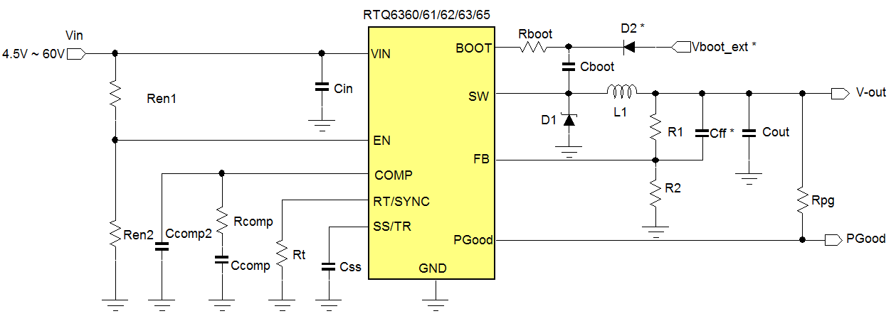
Figure 1 (parts with * are optional, PGood and Softstart are only available on DFN packages)
The following guidelines can be used to calculate the various application components. For convenience, Richtek has developed an Excel calculation sheet which makes the design and component choice easy and quick. The RTQ29xx and RTQ63xx excel tools can be downloaded here and here.
- Switching frequency considerations:
Since this family can work over a wide input voltage range, the converter switching frequency is an important parameter: For applications with input voltages higher than 24V, a moderate switching frequency (< 1MHz) is recommended to reduce switching losses. The RTQ29xx/RTQ63xx IC control circuit will start to reduce its frequency when the high-side switch minimum on-time or minimum off-time are reached, but in doing so, the converter output ripple will increase. If the application needs to work over a wide input voltage range with low output ripple, the switching frequency may need to be reduced to maintain the operation within the maximum and minimum duty-cycle limitations.
The frequency can be set via the external RT resistor: For RTQ6360/61/62:  ; For RTQ6363/65:
- Input and output voltage considerations:
The RTQ29xx/RTQ63xx output voltage can be adjusted from 0.8V to VIN by means of R1 and R2:
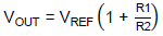 where VREF = 0.8V
The impedance of the feedback network is not critical, but it is recommended to avoid too high resistor values to reduce sensitivity to noise. It is recommended to keep the value of R2 below 80kΩ.
RTQ29xx/RTQ63xx series has a typical minimum on-time of 100nsec, achieving minimum duty-cycle in CCM mode of 100nsec*FSW.
RTQ29xx/RTQ63xx series has a typical minimum off-time of 130nsec, achieving maximum duty-cycle in CCM mode of 1-130nsec*FSW. So a 1MHz switching frequency would give a minimum duty-cycle of 10% and a maximum duty-cycle of 87%. It is possible to run the converter outside its minimum and maximum duty-cycle range, at the expense of increased output ripple.
When operating RTQ29xx/RTQ63xx series in high duty-cycles exceeding 65% or input voltage below 5.5V the external bootstrap supply via D2 should be added. The external bootstrap supply is recommended to be 5V, using a normal diode for D1. When lower bootstrap supply is used, D2 should preferably be a small Schottky diode)
- For Inductor value of L1 there are two main criteria that need to be considered: Inductor current ripple and slope compensation. For applications with duty-cycle lower than 50%, the inductor can be calculated to provide a ripple current of 20 ~ 30% of the IC rated current: (so for 5A converter RTQ6365, DIL would be around 0.3*5A = 1.5A even if the maximum application current is lower)
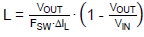 .
.
In applications where the duty-cycle can exceed 50%, the inductor current falling slope dI/dt also needs to fit the converter internal slope compensation: L1 value needs to fulfill the following criteria:  where slope compensation constant XC is: 0.5 for RTQ6360, 1.3 for RTQ6361, 2.1 for RTQ6362, 2.9 for RTQ6363, 4 for RTQ6365. For high input voltage supplies, wire wound shielded ferrite inductors are recommended.
- For output capacitor selection, there are several considerations:
a. Output ripple in CCM mode
Output ripple in CCM mode can be calculated from 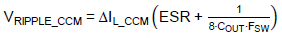
The CCM mode inductor ripple can be calculated from: 
When using ceramic output capacitors in these low voltage supplies, output ripple voltage in CCM mode will be small.
It should be noted that the output ripple in PSM mode would normally be higher than in CCM mode. Since PSM ripple is rather hard to calculate accurately, the designer needs to verify this behavior in the end-application at light loads.
b. Voltage sag during load transients
The voltage sag during a load transient in CCM mode depends on the load step, control loop speed and output capacitor. An approximate formula for voltage sag during a fast load step is shown below:
where DISTEP is the load step amplitude and FBW is the converter control bandwidth. Note that load step transitions between PSM and CCM mode operation will show higher voltage sag, because there is around 1% DC voltage difference between PSM mode and CCM mode. Converter bandwidth is normally set around 1/5 ~ 1/10 of the switching frequency, but the absolute value should stay below 80kHz. The converter bandwidth can be set via compensation resistor RCOMP.
- Input capacitor considerations:
The input capacitor will act as a storage buffer to provide the high frequency switching current peaks of the converter. The input capacitor should be chosen to provide adequate filtering of the converter input, to minimize the VIN high frequency ripple. Low ESR ceramic input capacitors should be placed close to the converter VIN pin and the Schottky diode ground connection. At high input voltages, ceramic capacitors will have severely reduced capacitance, which should be considered when calculating the input ripple voltage. The peak-peak input ripple voltage can be approximated by:
 where
where  and CIN is the effective capacitance at the DC input voltage.
It is recommended to keep the input ripple voltage below 1.3Vpp.
For higher than 50V input supply, normally one or several 2.2µF/100V 1206 size MLCC capacitors will be needed depending on application load current.
For higher current converters the input capacitor RMS current rating should also be checked:
 The maximum RMS current will happen when VOUT is 50% of VIN.
If the converter requires hot-plugging into live input supplies, it is recommended to add an electrolytic capacitor (e.g. 47µF/100V) in parallel with the ceramic input capacitor.
- Calculation of compensation components:
The RTQ29xx/RTQ63xx series compensation can use standard current mode type II compensation. The below simple formulas can be used:
The compensator gain is set by RCOMP, and the value is calculated to provide a suitable converter crossover frequency (FC around 0.05 ~ 0.1*FSW). 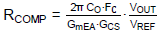 . Note that FC should not exceed 80kHz.
For higher input voltage supplies and supplies using electrolytic output capacitors it is recommended to use moderate bandwidth values.
The value of CCOMP is selected to set the compensation zero 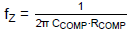 a bit below the converter load pole
 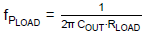 where RLOAD = VOUT / IOUT.
The value for CCOMP2 is chosen to set the high frequency pole at the output capacitor ESR zero: 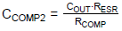
When ceramic output capacitors are used, the ESR zero will lie at very high frequencies, above the converter switching frequency. In this case, choose CCOMP2 for a high frequency pole at half the switching frequency: 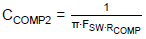
The feed-forward capacitor CFF in parallel with the upper feedback resistor is normally not needed for improving control loop response. But some small CFF capacitor in parallel with the upper feedback resistor can sometimes improve the PSM operation; by injecting some extra ripple on the FB pin, PSM double pulsing can be reduced. This can be tested case by case. Be careful when adding CFF as it can push the converter bandwidth to high values, reducing the gain margin and leading to unstable behavior.
- RTQ29xx/RTQ63xx are asynchronous buck converters and need an external Schottky diode to conduct the inductor current when the high-side MOSFET is off. The Schottky diode should have sufficient voltage rating (≥ VIN_MAX) and the forward voltage drop should be low to minimize power loss. The forward voltage drop should also be low enough to avoid current flow in the IC internal small low-side MOSFET body diode. The RTQ29xx/RTQ63xx datasheets provide graphs with maximum allowed forward voltage drop over temperature. To minimize switching losses, the Schottky diode junction capacitance and reverse recovery effects should be minimized. Finally the Schottky diode reverse leakage current at maximum reverse voltage and maximum ambient temperature should be checked, as high leakage current can lead to excessive diode dissipation and potential thermal runaway.
- The soft-start capacitor (DFN packages only) sets the time tSS from EN high to VOUT reaching its final value which is defined by
 . CSS is the value of the soft-start capacitor and ISS is the soft-start current (typically 6µA). VOUT starts rising when the VSS ramp passes 0.3V, and ends when VSS ramp passes 1.1V.
The VOUT rise time can therefore be calculated by:  .
.
Supplies with high output voltage and/or large value output capacitors should use sufficient soft-start time to avoid high inrush currents. Generally the soft-start time should be long enough to ensure the output capacitor can be fully charged without hitting the converter current limit. For PSOP-8 package versions, the soft-start time is internally fixed at 2msec.
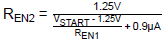
- The converter can be enabled by pulling high the EN pin. The EN rising threshold is typically 1.25V. A fixed 0.9µA internal current source will enable the converter in case of floating EN pin. When the EN pin passes the EN rising threshold, an additional 2.9µA internal current source will be enabled, and totally 3.8µA will flow out of the EN pin.
By connecting the EN pin via a resistor divider REN1 and REN2 between VIN and ground, the part can start and stop at specific VIN values: 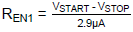
The EN pin is 60V tolerant.
- The PGOOD pin (DFN packages only) signal can be used to monitor the output voltage. It is an open drain output and can be pulled up to an external voltage or the output voltage. To minimize switching noise pick-up, it is recommended to use 1k ~ 10kΩ pull-up resistors to reduce the chance of switching noise pick-up. The PGOOD pin is 60V tolerant.
3.
First Example application: 3.3V/0.5A output
In this first example we will design a low current 3.3V MCU supply with a wide input voltage range from 12V to 60V, with a nominal value of 48V. This is a typical industrial MCU power supply example. We will use the RTQ63xx excel tool to show the step by step design.
The 60V maximum input voltage and the 0.5A max load current makes RTQ6360 the obvious choice. To provide a supply ready signal (Pgood) for the MCU, we will choose the DFN version RTQ6360GQW for this design. We will set the start-up voltage at 10V and shut-down voltage at 8V. The CCM output ripple should be less than 1% of the output voltage, and voltage sag during 0.2A to 0.5A load transient less than 5% of Vout. Figure 2 shows the Excel design tool input parameter section.
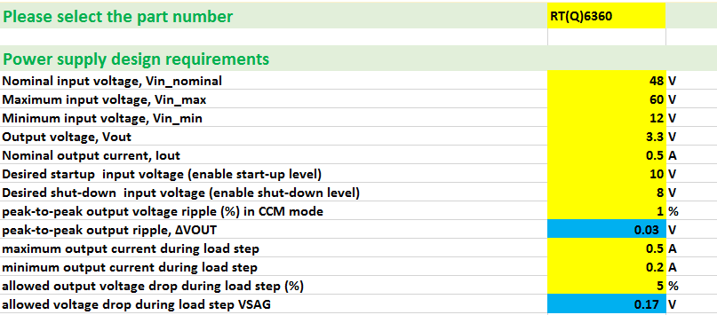
Figure 2
The first step in the design is to select the switching frequency. The excel tool will calculate the maximum switching frequency based on maximum input voltage, output voltage and minimum on-time. It will also calculate the maximum switching frequency based on output short-circuit condition: This is related to the minimum duty-cycle that the converter is able to achieve in output short-circuit with frequency fold-back. For this design, we’ll set the frequency at 400kHz which will satisfy both conditions. See figure 3.

Figure 3
Next step is the inductor value calculation: For this design we will set the inductor ripple current at 30% of the IC rated current. The design tool will calculate the inductor value based on this ripple current. It will also calculate the minimum required inductance to satisfy the converter slope compensation requirement. We will choose 47uH inductance, which should have a saturation current that is higher than 0.58A.
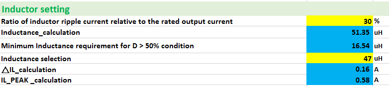
Figure 4
For this design, a Würth Electronic WE-LQS 74404052470 type was choosen. Figure 5 shows the specifications.
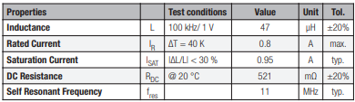
Figure 5
The next step is the input capacitor selection. The design tool will calculate the required effective input capacitance to keep the peak-peak input voltage ripple lower than 1.3Vpp at worst case input voltage and output current.
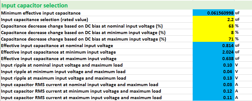
Figure 6
For this design, a single 2.2µF/100V MLCC capacitor HMK316AC7225KL-TE was chosen. Since the effective capacitance highly depends on input DC voltage, we should enter the capacitance decrease rate at nominal, minimum and maximum input voltage: The capacitance decrease over DC bias can be found from the capacitance characteristics datasheet, see figure 7 left side. The design tool will then calculate the effective input capacitance and the expected input voltage ripple at each input voltage. It will also calculate the maximum RMS current in the input capacitor. You can then check the temperature rise of the capacitor at this condition (figure 7 right side). In this design the RMS ripple current is very small and hardly leads to any dissipation in the capacitor.
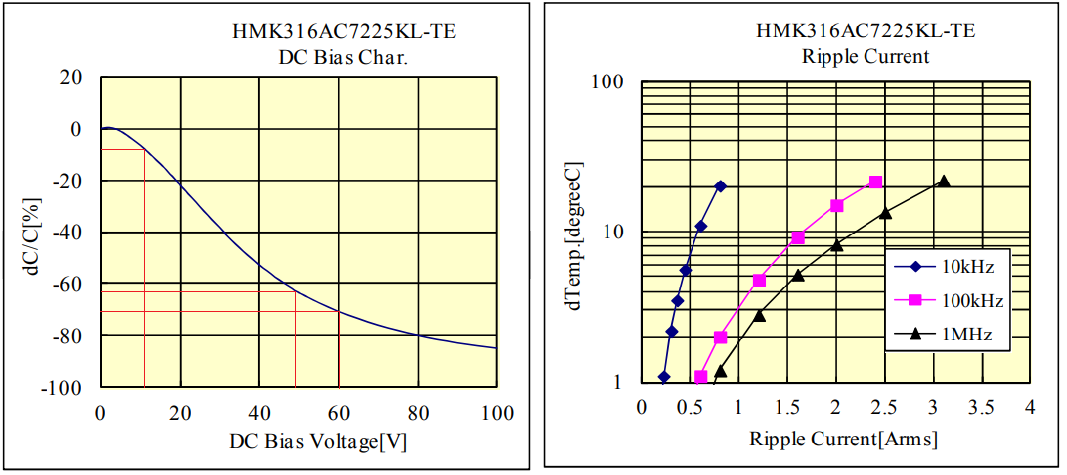
Figure 7
The next step is the output capacitor selection. Its value will determine the output voltage ripple and the voltage sag during load transient at a given load step and converter control bandwidth. For this design we’ll set the control bandwidth at 10% of the switching frequency. The load step voltage sag requirement will now define the minimum required effective output capacitance value, which is 7.26μF.
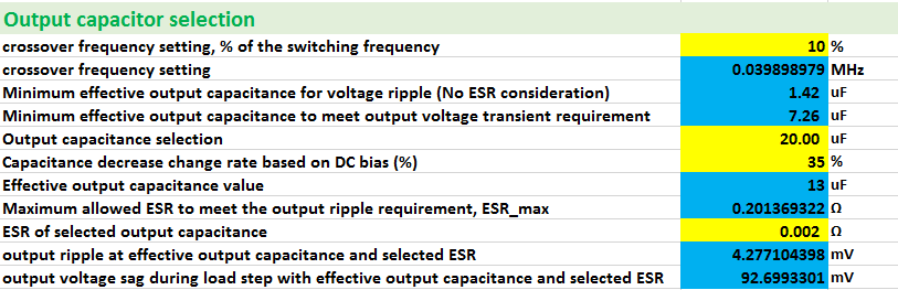
Figure 8
For this design, two small size 10µF/16V X5R 0805 EMK212ABJ106KG capacitors were chosen. It is very important to include the capacitance decrease due to DC bias as well (see figure 9), as it will affect output ripple, voltage sag and converter stability. After the rated capacitance and capacitance % decrease at 3.3V DC bias has been entered in the design tool, it will calculate the effective total output capacitance, the minimum required ESR to meet the output ripple specification, and the actual output ripple and voltage sag.
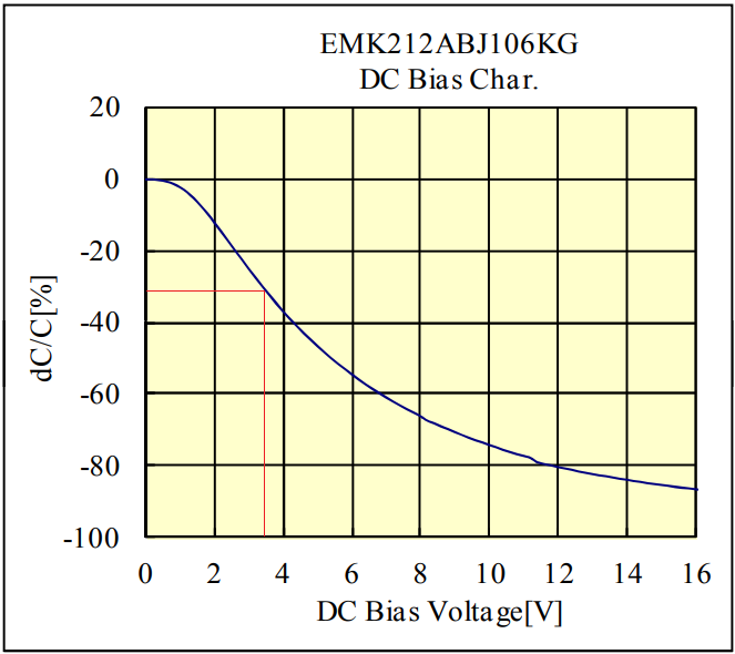
Figure 9
Next step is the Freewheel diode selection. The RTQ29xx/RTQ63xx series require an external Schottky diode to provide a current path for the inductor current when the high-side MOSFET is off. The forward drop of the Schottky diode should be low, to reduce the power loss in the diode, but also to avoid current flow in the IC internal small low-side MOSFET that is used for boot strap capacitor re-charge in light load. (see figure 10). This means that the forward voltage drop of the Schottky diode at maximum load current should be low compared to the body diode of the IC internal low side MOSFET. For Schottky diodes this is normally not a problem.
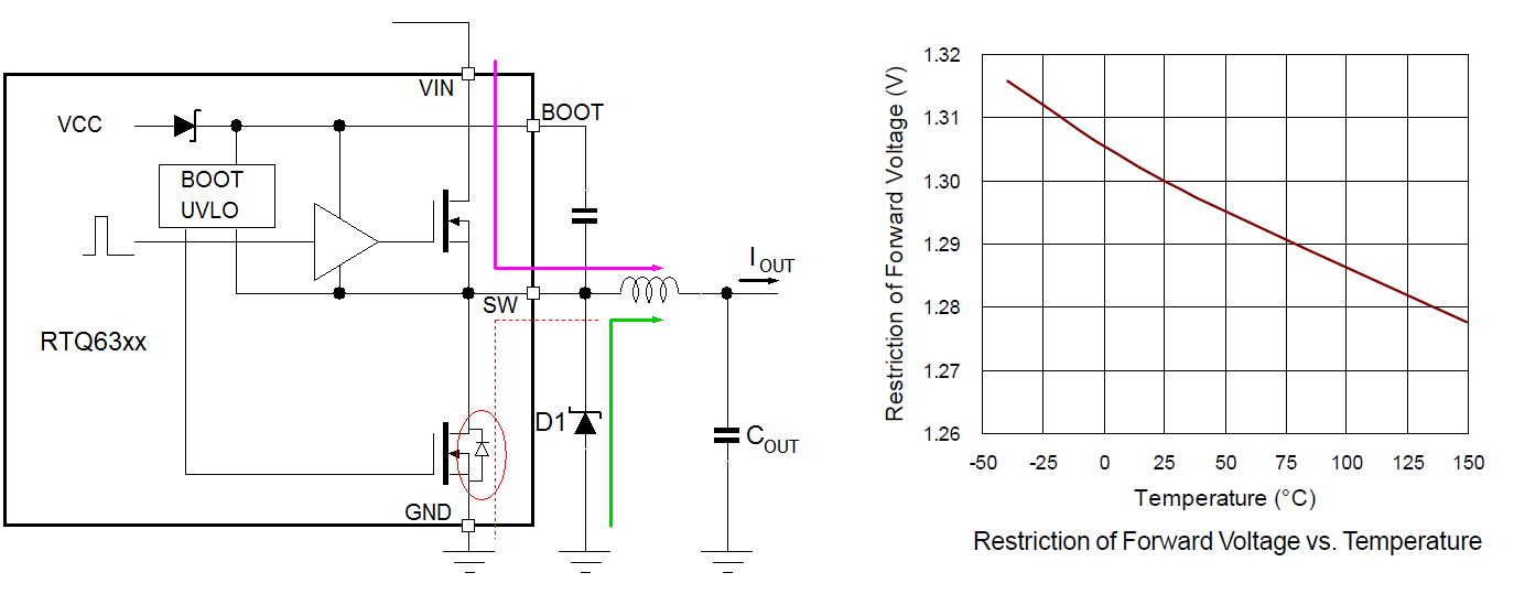
Figure 10
For this low current supply, switching losses will be a major part of the total losses. The Schottky diode capacitance and reverse recovery effects should be minimized. Finally, since this supply can work with input voltage up to 60V, the Schottky diode voltage rating should be sufficient, and reverse leakage current at maximum reverse voltage and maximum ambient temperature should be checked as well.
For this design a 60V/1A PMEG6010ER Schottky diode was chosen. The important parameters are shown in figure 11.
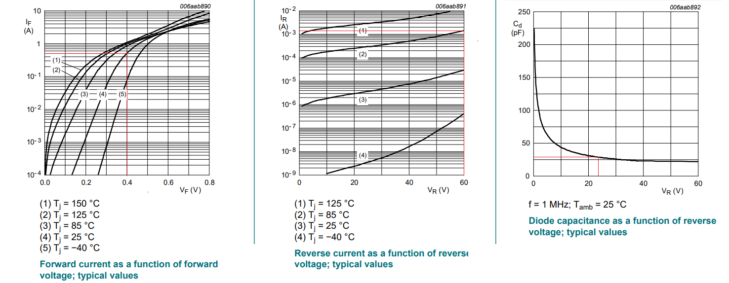
Figure 11
The PMEG6010ER forward voltage at 25°C and 0.5A is 0.4V and the diode worst case forward voltage values will not come close to the limit values as shown in the RTQ6360 datasheet. At 85°C ambient and 60V reverse voltage, the reverse leakage current is 1.3mA. The power loss due to leakage current is D*VIN*ILEAKAGE = 0.055*60*0.0013 = 4mW, which will not have much impact on the converter efficiency and will not cause thermal runaway. The Schottky diode junction capacitance is highly dependent on diode reverse voltage. This capacitance influences the IC internal high-side MOSFET switching losses, so lower capacitance Schottky diodes will reduce the switching losses, especially at higher input voltages.
The calculation of the feedback resistors is straightforward: the designer inputs the low-side feedback resistor and the tool calculates the high-side resistor.
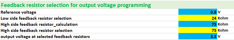
Figure 12
The calculation of the compensation resistor RCOMP is based on the previously entered converter bandwidth, the effective output capacitance and the IC parameters. CCOMP is then calculated to set the compensation zero to coincide with the converter load pole. For low ESR ceramic output capacitors, the CCOMP2 capacitors is calculated to set the compensator pole at half the switching frequency. Please note that RTQ6360 COMP pin internally has 5.7pF to ground, so the external CCOMP2 value can be 5.7pF lower than the calculated one. See figure 13.
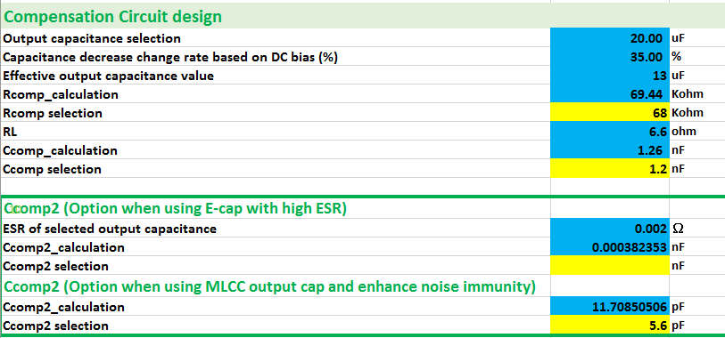
Figure 13
The design can be finalized with the calculation of the Enable resistor divider and Soft-start capacitor: With the entered VIN start and stop voltages, the design tool calculates the recommended upper REN1 resistor, and after entering the actual value, it calculates the second REN2 resistor and shows the actual start and stop levels based on the actual resistor values used.
The soft-start time for the 3.3V converter is not critical and we choose an arbitrary 3msec soft-start time, which requires a 10nF soft-start capacitor. The PGOOD pin is pulled up with a 4.7kΩ to VOUT. See figure 14.
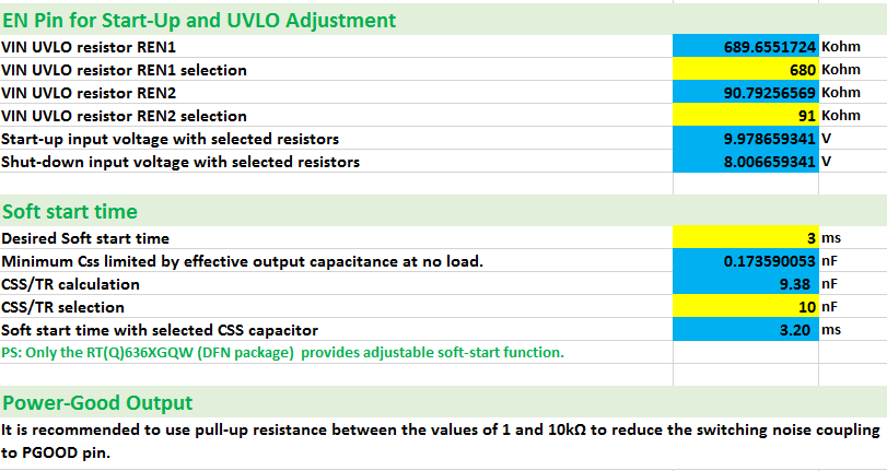
Figure 14
The complete application circuit and a PCB layout example is shown in figure 15.
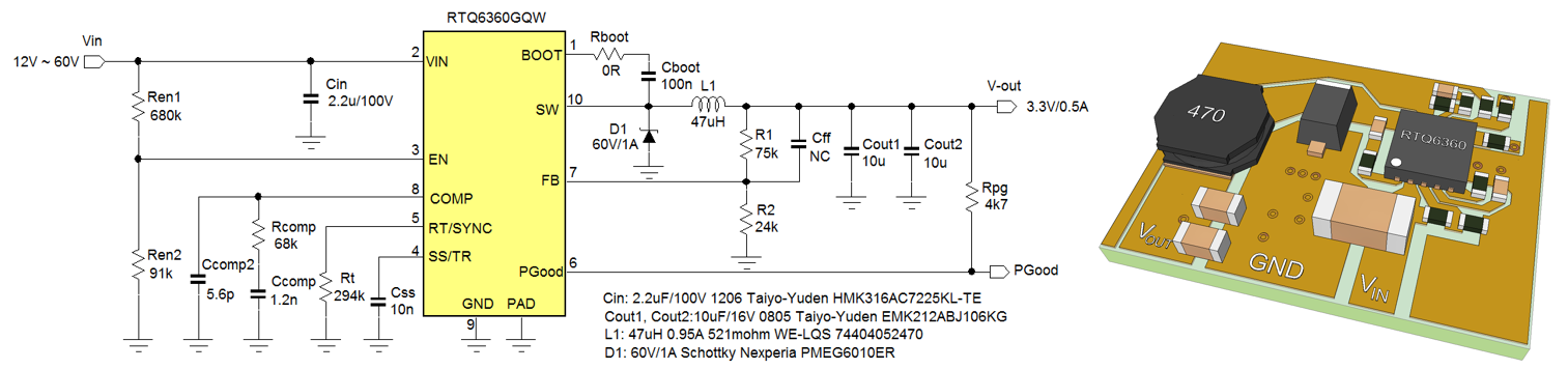
Figure 15
The circuit was built on the RTQ6360GQW evaluation board, and the all performance items were measured and compared with calculated values:
|
|
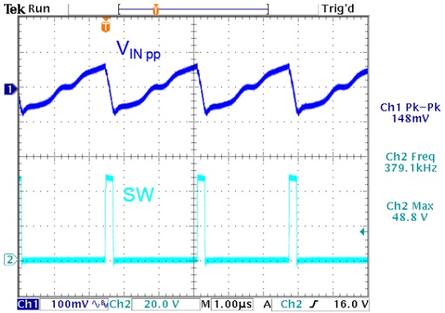
Measurement of input ripple at VIN = 48V, VOUT = 3.3V, 0.5A load
Calculated value: 100mVpp, measured value: 148mVpp
|
Figure 16
|
Output ripple in PSM mode VIN = 48V, VOUT = 3.3V, 1mA load
|
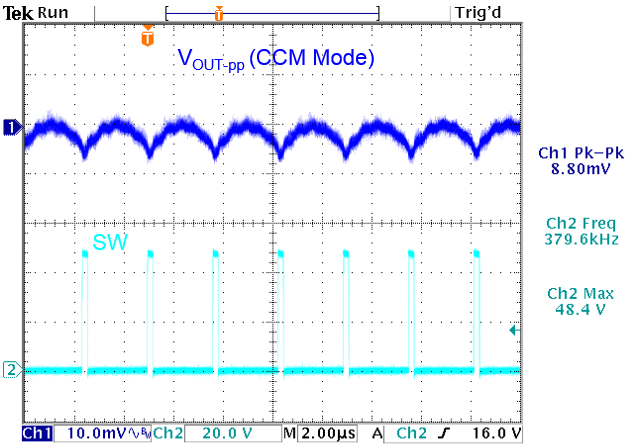
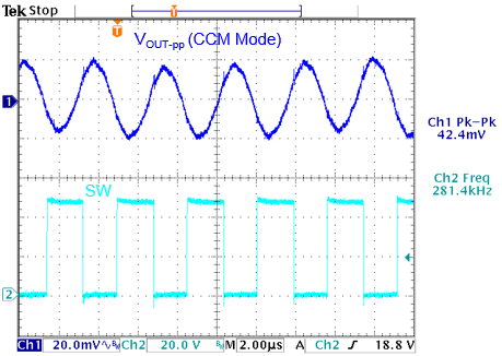
Output ripple in CCM mode VIN = 48V, VOUT = 3.3V, 0.5A load
|
|
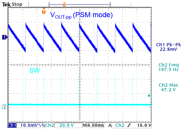
Figure 17
|
|
|
Measured value: 22.8mVpp
|
Calculated value: 4.3mVpp, measured value: 8.8mVpp
|
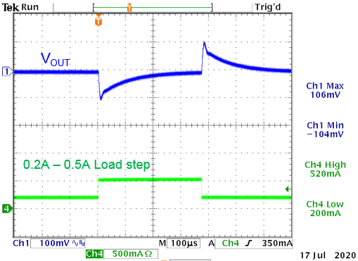
The converter voltage sag during load step was measured by using the Richtek Fast Load transient Tool.
|
VIN = 48V, 0.2A ~ 0.5A fast load step
|
VIN = 24V, 0.2A ~ 0.5A fast load step
|
|
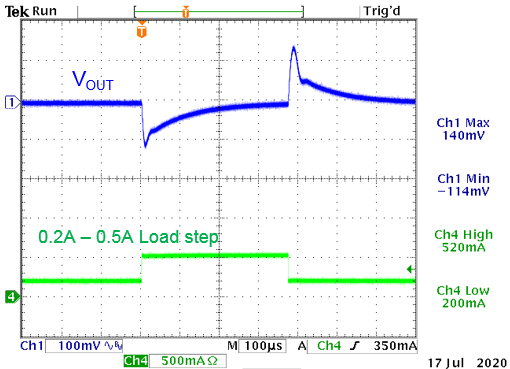
Figure 18
|
|
|
Calculated value:92mV; measured value: 114mV
|
Calculated value: 92mV, measured value: 104mV
|
The step load response at 48V input voltage in figure 18 left side is a bit different from the 24V input condition (figure 18 right side), especially the overshoot when load goes from 0.5A to 0.2A. During sudden load drop, the converter will try to quickly reduce its on-time. At 48V input, the converter is already working close to its minimum on time, so the headroom in on-time reduction is limited, hence resulting in larger overshoot. The step load in both cases shows a small ring, which points to lower phase margin.
A gain-phase measurement (figure 19) shows this more clearly:
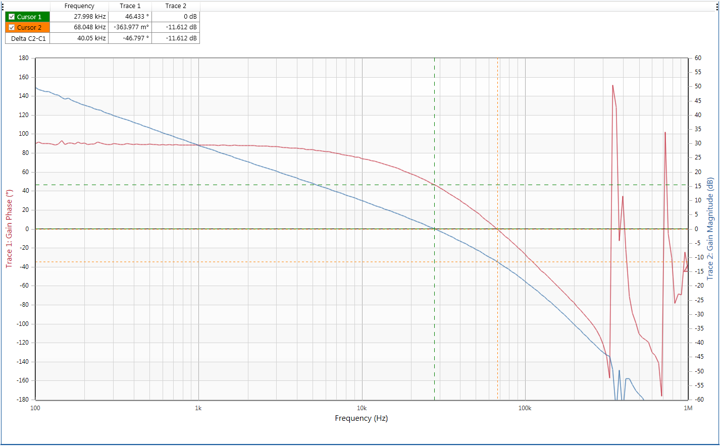
Figure 19 VIN = 48V, Vout = 3.3V / 0.5A load: Bandwidth = 28kHz, Phase margin 46 dgs
The gain-phase Bode plot shows that the loop phase drops quite fast above the crossover frequency. This can be slightly improved by removing the CCOMP2 capacitor of 5.6pF:
Figure 20 shows the gain-phase measurement result when CCOMP2 is removed: The phase margin is slightly better.
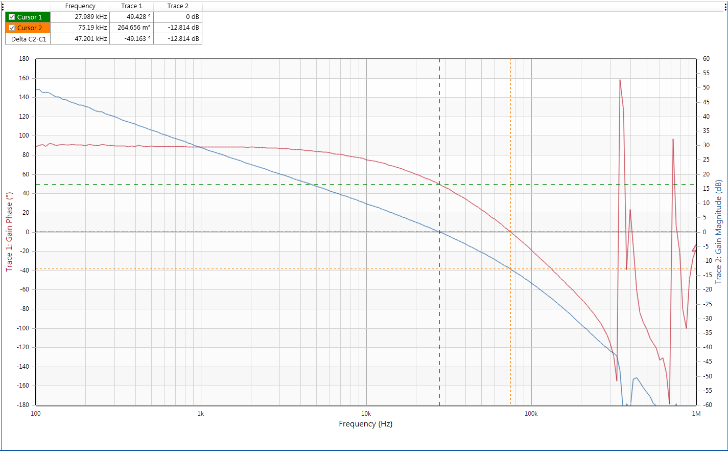
Figure 20 VIN = 48V, Vout = 3.3V/0.5A load and removed CCOMP2 capacitor: Bandwidth = 28kHz, Phase margin 49 dgs
If better phase margin is required, it is recommended to set the converter bandwidth frequency setting percentage at a lower value (e.g. 7% instead of 10% of FSW) at the expense of slightly larger voltage sag during load steps and re-calculating the RCOMP, CCOMP and CCOMP2 values.
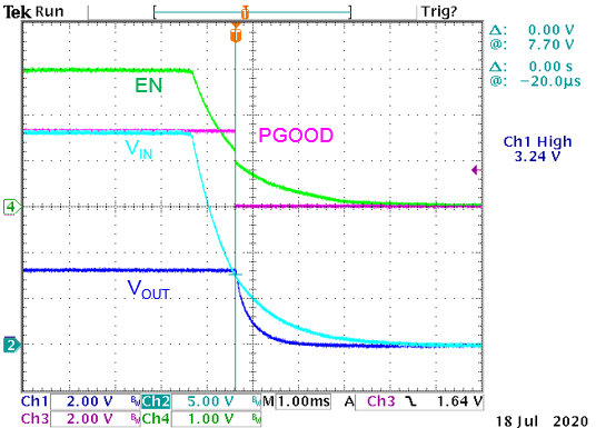
The converter start-up from VIN and Shut-down from VIN was also measured. The measurement results match the calculated values quite well. The small hysteresis step in the Enable signal can be seen when it passes the threshold. See figure 21.
|
Start-up at rising VIN:
|
Shut-down at falling VIN:
|
|
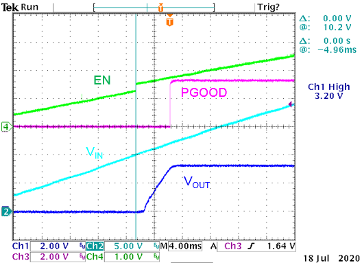
Figure 21
|
|
|
VSTART calculated: 10V; VSTART measured: 10.2V
|
VSTOP calculated: 8V; VSTOP measured: 7.7V
|
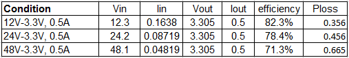
The converter efficiency was also measured at different input voltages: Figure 22 shows that the efficiency is highly dependent on the input voltage.
|
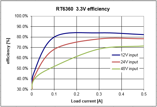
|
Since efficiency = POUT / (POUT + PLOSS) it is useful to analyze the power losses of the converter.
|
|
|
|
As can be seen, the total power losses at 48V input are almost double of the losses in 12V input condition, which is mainly caused by the higher switching losses at higher input voltage.
|
Figure 22
4.
Second Example application: 24V/3A (72W) output
In this second example we will design a 24V/3A converter running from an industrial 48V supply. This is a high power design and correct component selection is quite important.
For the IC selection we can either choose the RTQ6363 (3.5A version) or the RTQ6365 (5A) version). The RDSON of the 5A version is slightly better than the 3.5A version, but the 5A version has higher current limit, which means that an inductor with larger saturation current must be used. In this example, we will select the RTQ6363, and choose the DFN 4x4-package version RTQ6363GQW, which has better thermal resistance compared to the PSOP-8 package.
We will use the RTQ63xx excel design tool again to calculate the component values.
We will set the start-up voltage at 35V and shut-down voltage at 28V, which ensures clean start-up of the power supply. CCM output ripple should be less than 1% of the output voltage, and voltage sag during 1A to 3A load transient should be less than 5% of Vout. Figure 23 shows the Excel design tool input parameter section.
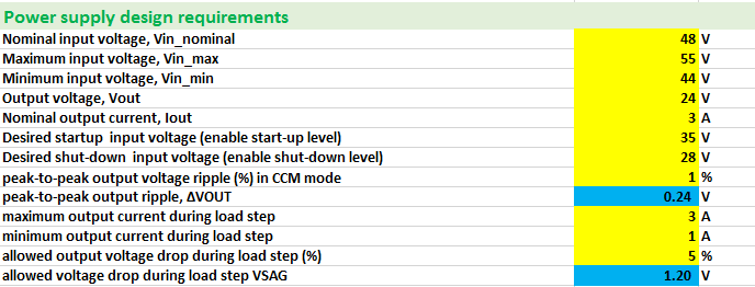
Figure 23
The first step in the design is to select the switching frequency. The excel tool will calculate the maximum switching frequency based on maximum input voltage, output voltage and minimum on-time, as well as the maximum switching frequency based on output short-circuit condition. As the duty-cycle for this 48V ~ 24V design lies around 50%, the minimum on-time will not easily be reached, allowing higher switching frequencies. But it is not wise to choose high switching frequencies for 48V input supplies as the switching losses will increase considerably. To minimize the switching losses, we will set the frequency at 300kHz. See figure 24.
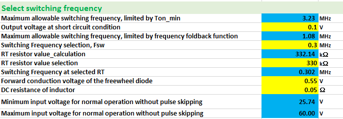
Figure 24
Next step is the inductor value calculation: With the selecting 30% ripple current, the design tool will calculate the inductor value based on this ripple current to be 38µH. The minimum required inductance to satisfy the converter slope compensation requirement is 27µH. We will choose 47µH inductance, which will give an 850mApp current ripple. The inductor saturation current should be higher than 3.4A and the RTQ6363GQW 5.5A peak current limit should also be considered when choosing the inductor saturation current.
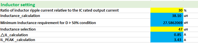
Figure 25
For this design, a Würth Electronic WE-PD 7447709470 type was choosen which has 4.5A saturation current. Figure 26 shows the specifications. Slight saturation during over-current situations is allowed.
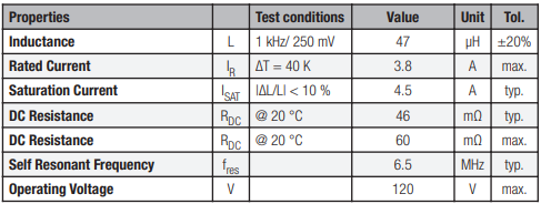
Figure 26
The next step is the input capacitor selection. The design tool will calculate the required effective input capacitance to keep the peak-peak input voltage ripple lower than 1.3Vpp at worst case input voltage and output current.
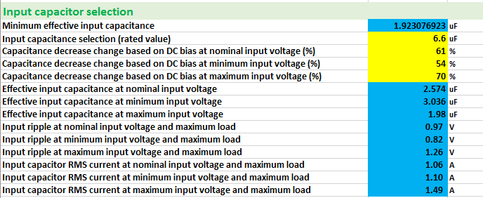
Figure 27
For this design, we will use three pieces 2.2µF/100V MLCC capacitors HMK316AC7225KL-TE in parallel to get sufficient capacitance at high input voltage. After we enter the capacitance decrease rate at nominal, minimum and maximum input voltage from the capacitor datasheet graph, the design tool will calculate the effective input capacitance and the expected input voltage ripple at each input voltage. It will also calculate the maximum RMS current in the input capacitor. As we use three capacitors in parallel, each capacitor will see 1/3 of the calculated RMS current so worst case RMS current in each capacitor is 0.5A. As you can see in figure 28 right side, the temperature rise of the capacitor at this condition is still small.
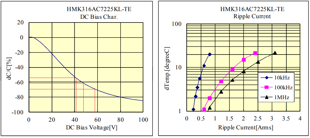
Figure 28
The next step is the output capacitor selection. Its value will determine the output voltage ripple and the voltage sag during load transient at a given load step and converter control bandwidth. For the high voltage and high power design moderate control bandwidth is recommended. We start with a control bandwidth of 10% of the switching frequency. The load step voltage sag requirement will now define the minimum required effective output capacitance value, which is 8.85μF.
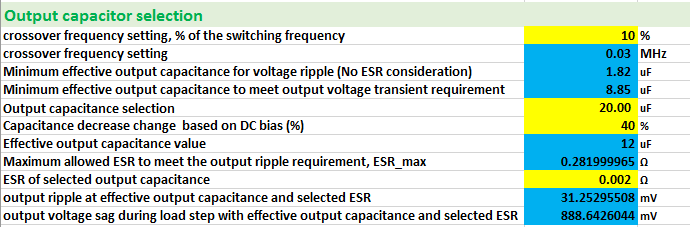
Figure 29
For this design, two 1210 size 10µF/50V X7S UMR325AC7106KM capacitors in parallel were chosen. It is very important to include the capacitance decrease due to DC bias as well (see figure 30), to ensure correct compensation calculation results. This capacitor type drops around 40% at 24Vdc. After the rated capacitance and 40% decrease at 24V has been entered, the design tool will calculate the effective total output capacitance, the minimum required ESR to meet the output ripple specification, and the actual output ripple and voltage sag.
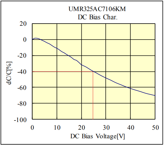
Figure 30
Next step is the freewheel diode selection. The total power dissipation in this design will be high, resulting in higher operation temperatures of the power components. It is therefore important to select parts that will operate reliably at high temperatures. With larger Schottky diodes, reverse leakage currents can be a critical parameter at high temperatures, and for this design we selected a Trench type 60V/5A PMEG060T050ELPE Schottky which exhibits lower reverse leakage current compared to normal planar Schottky diodes (1). The important parameters are shown in figure 31.
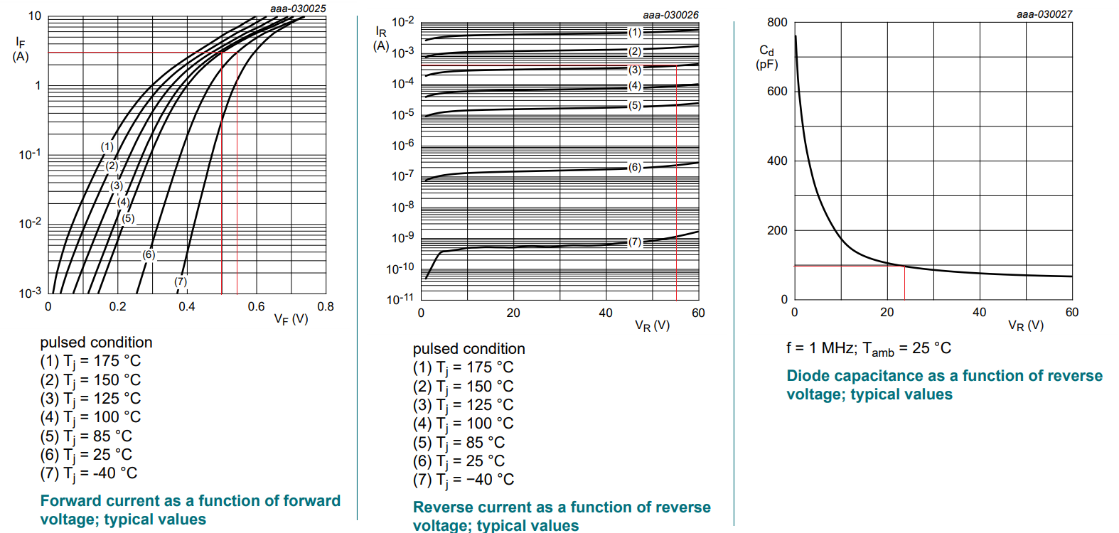
Figure 31
At 125°C ambient and 55V reverse voltage, the reverse leakage current is 0.4mA. The power loss due to leakage current is very low: D*VIN*ILEAKAGE = 0.45*55*0.0004 = 9.9mW.
The junction capacitance is highly dependent on diode reverse voltage. As this capacitance influences the IC internal high side MOSFET switching losses, Schottky diodes with lower capacitance can help reduce switching losses, although the reverse recovery charge of the diode will also play a role (1).
The PMEG060T050ELPE forward voltage at 25°C and 3A is 0.54V and the diode worst case forward voltage values will not come close to the limit values as shown in the RTQ6363 datasheet, so there is no risk of current flow in the body diode of the RTQ6363 small low side MOSFET. See figure 32.
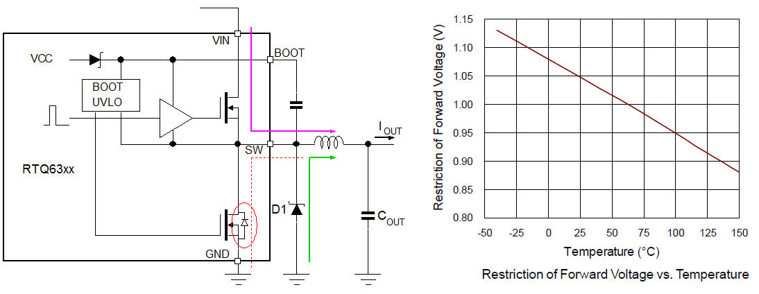
Figure 32
The calculation of the feedback resistors is straightforward: the designer inputs the low-side feedback resistor and the tool calculates the high-side resistor.
Figure 33
The calculation of the compensation resistor RCOMP is based on the previously entered converter bandwidth, the effective output capacitance and the IC parameters. CCOMP is then calculated to set the compensation zero to coincide with the converter load pole. For low ESR ceramic output capacitors, the CCOMP2 capacitors is calculated to set the compensator pole at half the switching frequency. Please note that RTQ6363 COMP pin internally has 26pF to ground, so the external CCOMP2 value can be 26pF lower than the calculated one. See figure 34.
Figure 34
The 48V to 24V design duty-cycle does not reach 65%, so the external bootstrap charge circuit is not needed.
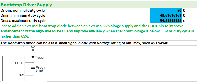
Figure 35
Finally the Enable resistor divider and Soft-start capacitor can be calculated. As the effective output capacitance (12µF) is relatively low the inrush current during soft-start is also low. We choose the 3msec soft-start time again, which requires a 10nF soft-start capacitor. See figure 36.
The PGOOD pin in this example is pulled up with a 10kΩ to VOUT, but for power sequencing it could be pulled up to an external low voltage supply or apply a resistor divider from VOUT.
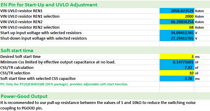
Figure 36
The complete application circuit and a PCB layout example is shown in figure 37.
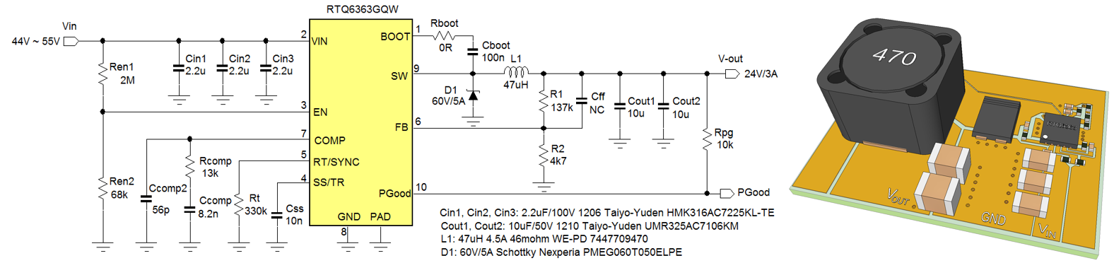
Figure 37
The circuit was built on the RTQ6363GQW evaluation board, and the all performance items were measured and compared with calculated values:
|
Input ripple measurement at VIN = 48V, VOUT = 24V, 3A load
|
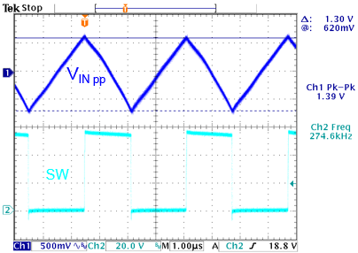
Input ripple measurement at VIN = 55V, VOUT = 24V, 3A load
|
|
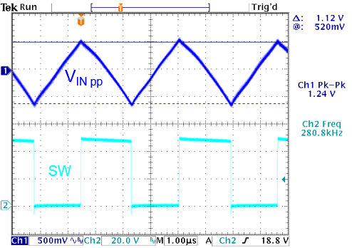
Figure 38
|
|
|
Calculated value: 0.97Vpp, measured value: 1.12Vpp
|
Calculated value: 1.26Vpp, measured value: 1.30Vpp
|
|
Output ripple in PSM mode VIN = 48V, VOUT = 24V, 1mA load
|
Output ripple in CCM mode VIN = 48V, VOUT = 24V, 3A load
|
|
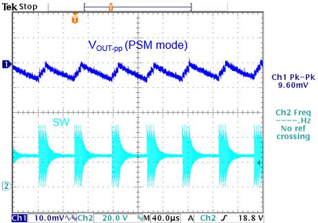
Figure 39
|
|
|
Measured value: 9.6mVpp
|
Calculated value: 32mVpp, measured value: 42mVpp
|
The converter voltage sag during load step was measured by using the Richtek Fast Load transient Tool.
|
VIN = 48V, 1A ~ 3A fast load step
|
VIN = 48V, 1A ~ 3A fast load step estimate bandwidth:
|
|
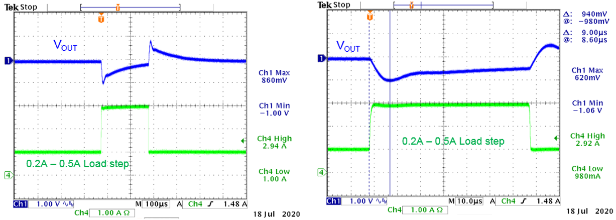
Figure 40
|
|
Vsag calculated value:0.88V; measured value: 1.0V
|
Response time = 9μsec. BW ≈ 0.3/9μsec = 33kHz
|
The step load shows a small ring, which points to lower phase margin. A gain-phase measurement (figure 41) shows this more clearly:
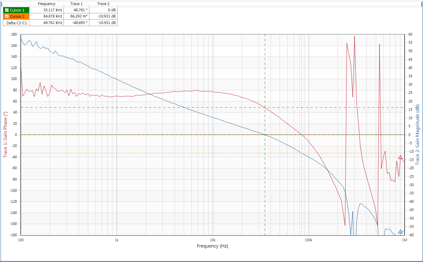
Figure 41
At VIN = 48V, and 24V with 3A load, the bandwidth shows 35kHz and phase margin is 48dgs. Gain margin is 11dB.
But when measuring gain-phase at 1A load the phase margin became worse:
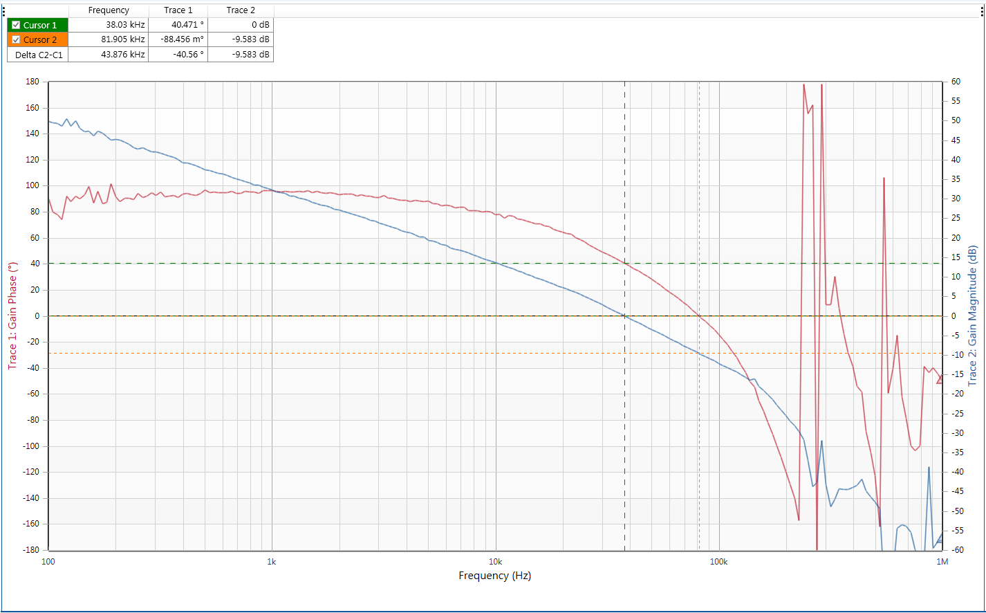
Figure 42
At VIN = 48V, and 24V with 1A load, the bandwidth shows 38kHz and phase margin is 41dgs. Gain margin is 9.6dB.
This phase margin is not sufficient and should be improved. Adding a small feed-forward capacitor CFF can boost the phase but it will also increase the bandwidth and lower the gain margin:
Figure 43 shows the gain-phase measurement result when 22pF CFF is added in parallel with the upper feedback resistor.
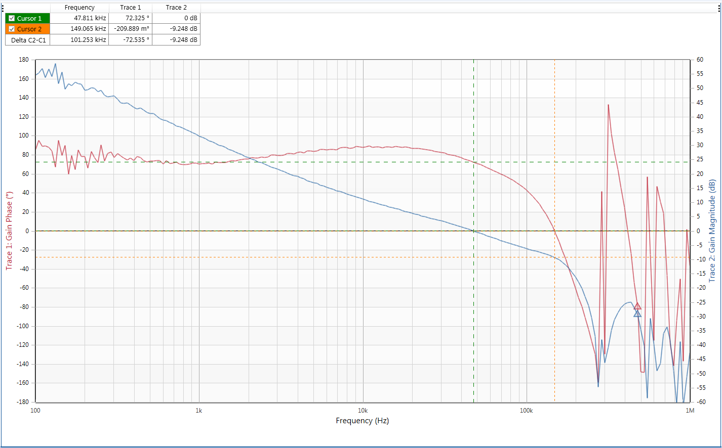
Figure 43
At VIN = 48V, and 24V with 1A load and added 22pF CFF, the bandwidth shows 48kHz and phase margin is 72dgs. But the Gain margin is only 9.2dB which is rather low.
A more stable design can be achieved by reducing the converter bandwidth; Figure 44 shows the gain-phase measurement when using a BW setting of 6% of the switching frequency. RCOMP = 7.5k, CCOMP = 12nF and CCOMP2 = 100pF, and no CFF.
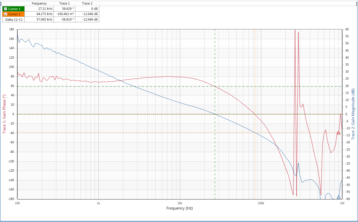
Figure 44
At VIN = 48V, and 24V with 1A load and compensation for 6% BW setting, the bandwidth shows 27kHz and phase margin is 58dgs. Gain margin is 13dB. This is a more stable design.
Due to the lower bandwidth setting, the load step voltage sag will become larger, but the step load response is without ring.
|
VIN = 48V, 0.2A ~ 0.5A fast load step
|
VIN = 48V, 1A ~ 3A fast load step estimate bandwidth:
|
|
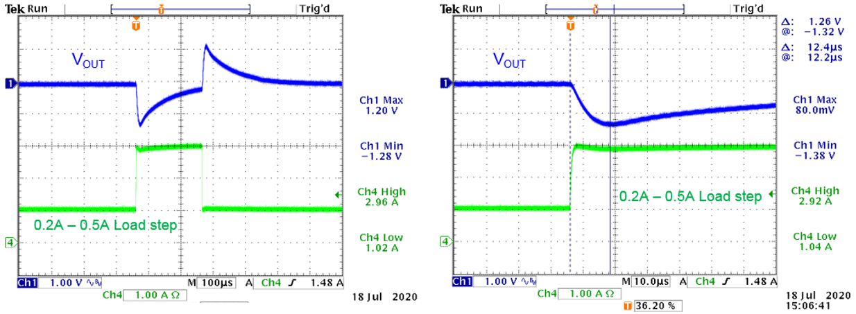
Figure 45
|
|
Calculated value:1.4V; measured value: 1.3V
|
Response time = 12.4μsec. BW ≈ 0.3/12.4μsec = 24kHz
|
The converter start-up from VIN and Shut-down from VIN were also measured. The small hysteresis step in the Enable signal can be seen when it passes the threshold. See figure 46.
|
Start-up at rising VIN:
|
Shut-down at falling VIN:
|
|
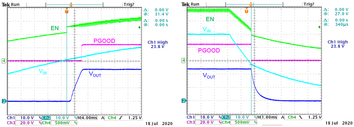
Figure 46
|
|
START calculated: 34V; VSTART measured: 31.4V
|
VSTOP calculated: 27.2V; VSTOP measured: 27V
|
The converter efficiency and power loss was also measured, see figure 47.
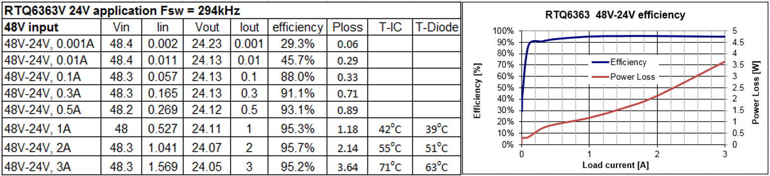
Figure 47
The total power loss at 3A load is 3.6W: Please note that the IC, Schottky diode and inductor all dissipate power so the heat is distributed as well. The IC however dissipates the majority of power and its thermal pad should be connected to sufficient copper on top layer and with thermal vias to inner layers and bottom layer.
5.
Schottky diode selection: Reverse leakage
current
In the original 48V – 24V/3A design, we had selected a special Trench type Schottky diode, which has greatly reduced reverse leakage current compared to standard Planar Schottky diodes (1). With the Trench type Schottky diode, the power loss due to leakage is extremely small. To show the differences between these two types of diodes in this high power design, we will also test the Nexperia PMEG060V050EPDZ Planar Schottky diode. The reverse leakage current graphs of the Trench and Planar type Schottky diodes are shown in figure 48.
|
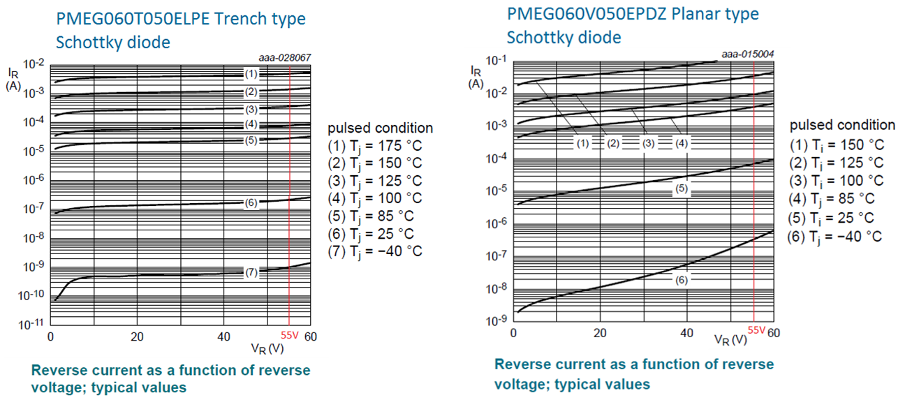
Figure 48
|
|
At maximum 55V input voltage and 100°C, the reverse leakage current is 80μA.
Reverse leakage Power loss = D*VIN*ILEAKAGE = 0.5*55V*80μA = 2mW
|
At maximum 55V input voltage and 100°C, the reverse leakage current is 10mA.
Reverse leakage Power loss = D*VIN*ILEAKAGE = 0.5*55V*10mA = 275mW
|
|
At 125°C, the reverse leakage current is 350μA.
Reverse leakage Power loss = 0.5*55V*350μA = 10mW
|
At 125°C, the reverse leakage current is 34mA. Reverse leakage Power loss = 0.5*55V*34mA = 0.935W
|
The calculations show that the reverse leakage current of a standard planar Schottky diodes can result in higher power loss in the diode at high temperatures.
This was verified by measurements: The two diodes were tested in the same 24V/3A application with 55V input, and the ambient temperature was gradually increased. Initially the Planar Schottky diode has slightly less power loss as its forward voltage is lower than the Trench type Schottky. But above 105°C, the power loss of the Planar Schottky increases rapidly, and at around 115°C it rises by itself and the diode fails at around 125°C due to excessive dissipation. See figure 49.
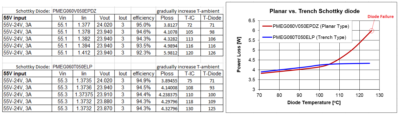
Figure 49
This example shows that Schottky diode reverse leakage current can be a critical parameter for application reliability.
6.
Conclusion
The RTQ63xx family can be used successfully in a wide range of step-down converter applications. The RTQ63xx excel design tool makes it easy to calculate the external components, and the measured performance matches the calculated values quite well. It is recommended to check the stability by means of gain-phase analysis although a fast step load test can also be used to quickly check stability aspects. For higher duty-cycle and high input voltage applications, the Schottky diode capacitance, and reverse leakage current are important parameters that must be considered.
References:
(1)Benchmarking of a Novel SiGe Diode Technology for the Usage in High Frequency 48V/12V Converter applications by A. Aneissi, M.Meissner, K.F. Hoffmann, R. Behtash, J. Fisher, S. Fahlbusch