Purpose
The RT5047 is a highly integrated voltage regulator and interface IC, specifically design for supplying power and control signals from advanced satellite set-top box (STB) modules to the LNB down-converter in the antenna dish or to the multi-switch box. This document explains the function and use of the RT5047 evaluation board (EVB), and provides information to enable operation, modification of the evaluation board and circuit to suit individual requirements.
Introduction
General Product Information
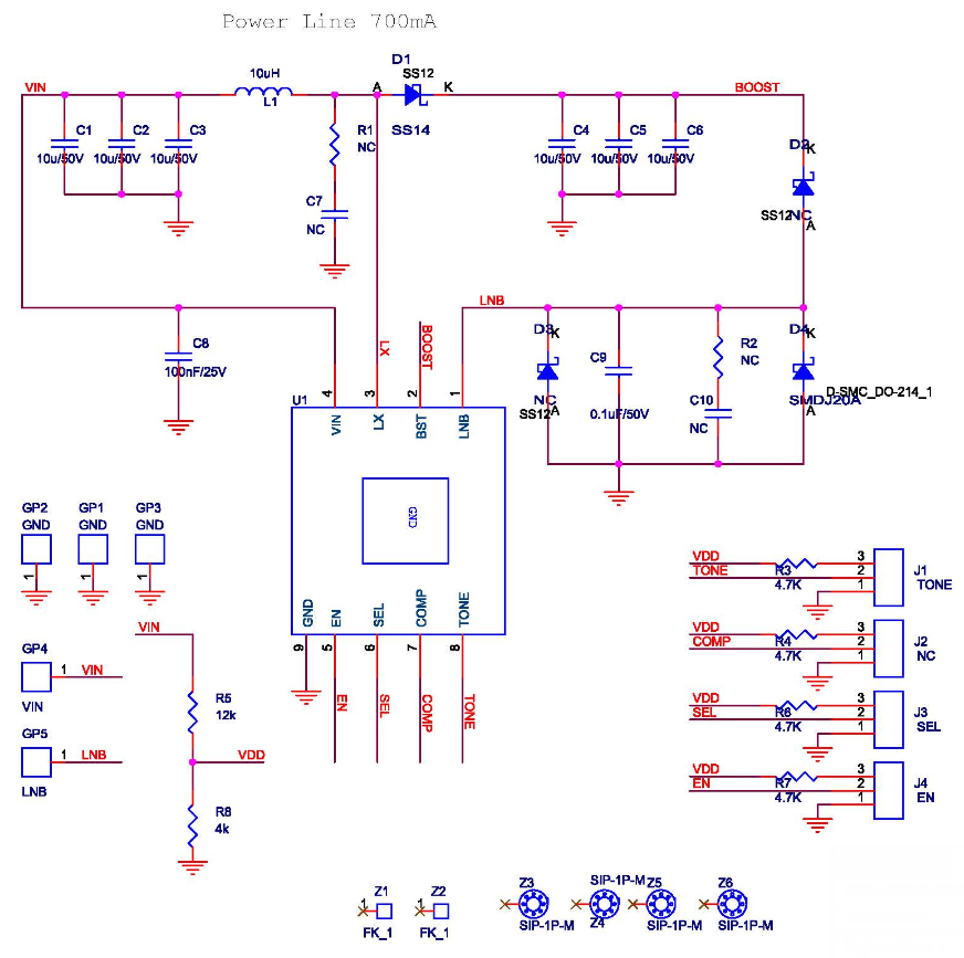
The device is consists of the independent current-mode boost controller and low dropout linear regulator along with the circuitry required for 22kHz tone shaping to support DiSEqC™ 1.x communications. The RT5047 provides fault protections including over-current, over-temperature and under-voltage lockout.
The RT5047 is available in a SOP-8 (Exposed Pad) package to achieve optimized solution for thermal dissipation.
Product Feature
-
Wide Input Supply Voltage Range : 8V to 16V
-
Output Current Limit of 550mA with 45ms timer
-
Low Noise LNB Output Voltage (13.3V and 18.3V by SEL Pin)
-
±3% High Accuracy for 0mA to 500mA Current Output
-
Push-Pull Output Stage minimizes 13.3V to 18.3V and 18.3V to 13.3V Output Transition Time
-
External 22kHz Tone Input
-
Meet DiSEqC™ 1.x Protocol
-
Output Short Circuit Protection
-
Over-temperature Protection
Key Performance Summary Table
|
Key Features
|
Evaluation Board Number : PCB014_V1
|
|
Default Input Voltage
|
12V
|
|
Max Output Current
|
500mA
|
|
Default Output Voltage
|
Low is for 13.3V, high is for 18.3V
|
|
Default Marking & Package Type
|
RT5047GSP, SOP-8 (Exposed Pad)
|
|
Operation Frequency
|
700kHz (Typ.)
|
Bench Test Setup Conditions
Headers Description and Placement
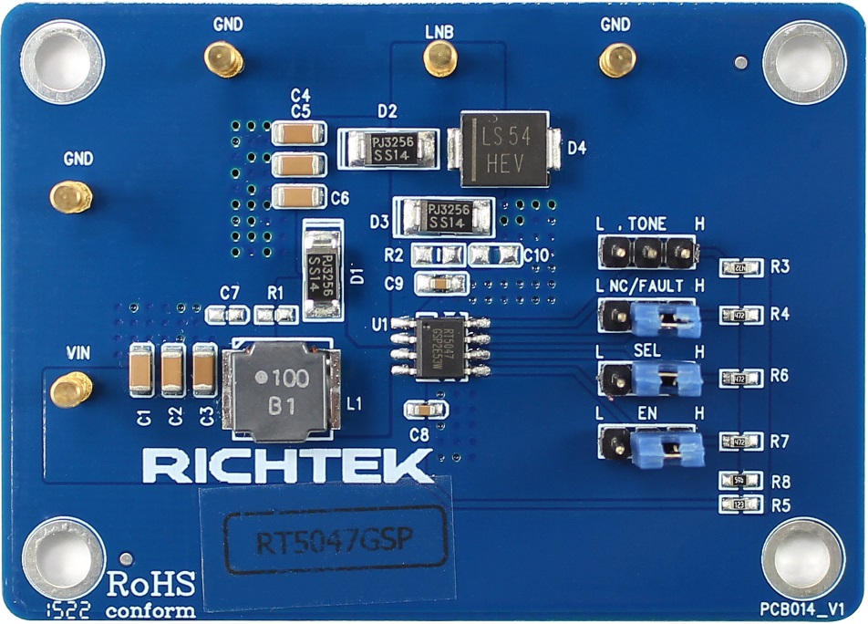
Please carefully inspect the EVB IC and external components, comparing them to the following Bill of Materials, to ensure that all components are installed and undamaged. If any components are missing or damaged during transportation, please contact the distributor or send e-mail to evb_service@richtek.com
Test Points
The EVB is provided with the test points and pin names listed in the table below.
|
Test point/
Pin name
|
Signal
|
Comment (expected waveforms or voltage levels on test points)
|
|
LNB
|
LNB output pin
|
Output Voltage for LNB.
|
|
BOOST
|
Boost feedback point
|
Boost Output and Tracking Supply Voltage to LNB.
|
|
LX
|
Switch node
|
Switching Node of DC/DC Boost Converter.
|
|
VIN
|
Input voltage
|
Power Supply Input.
|
|
EN
|
Enable point
|
High to enable the LNB and low to disable the LNB.
|
|
SEL
|
Output level select point
|
Low for VLNB is 13.3V and high for VLNB is 18.3V.
|
|
NC
|
No connection pin
|
Pull to 3.3V by 4.7kΩ resistor.
|
|
TONE
|
TONE input signal
|
Supply a 22kHz signal at this pin to control the output tone signal.
|
|
GND
|
Ground
|
The Exposed Pad must be soldered to a large PCB and connected to GND for maximum power dissipation.
|
Power-up & Measurement Procedure
1. Connect input power (8V < VIN < 16V) and input ground to VIN and GND test pins respectively.
2. To use a jumper at “H” option to tie EN test pin for enabling the device. Inversely, to use a jumper at “L” option to tie EN test pin and ground GND for disabling the device.
3. Supply a 22kHz signal of the “TONE” pin to adjust the output tone signal.
4. Verify the output voltage between LNB and GND.
5. Connect an external load up to 0.45A to the VOUT and GND terminals and verify the output voltage and current.
Schematic, Bill of Materials & Board Layout
EVB Schematic Diagram
Bill of Materials
|
Reference
|
Qty
|
Part Number
|
Description
|
Package
|
Manufacture
|
|
U1
|
1
|
RT5047GSP
|
Voltage Regulator
|
SOP-8
(Exposed Pad)
|
RICHTEK
|
|
C1, C2, C3, C4, C5, C6
|
6
|
|
10µF/50V
|
C-0805
|
|
|
C8
|
1
|
|
100nF/25V
|
C-0603
|
|
|
C9
|
1
|
|
0.1µF/50V
|
C-0805
|
|
|
C10
|
1
|
|
NC
|
|
|
|
R1, C7
|
2
|
|
NC
|
|
|
|
R2
|
1
|
|
NC
|
|
|
|
R3, R4, R6, R7
|
4
|
|
4.7k
|
R-0603
|
|
|
R5
|
1
|
|
12k
|
R-0603
|
|
|
R8
|
1
|
|
4k
|
R-0603
|
|
|
L1
|
1
|
|
10µH
|
L-NR8040_2
|
|
|
GP1, GP2, GP3
|
3
|
|
GND
|
SIP-1P-GP
|
|
|
GP4
|
1
|
|
VIN
|
SIP-1P-GP
|
|
|
GP5
|
1
|
|
LNB
|
SIP-1P-GP
|
|
|
D1, D2, D3
|
3
|
|
SS14
|
SS14
|
|
|
D4
|
1
|
|
SMDJ20A
|
D-SMC_DO-214_1
|
|
|
J1
|
1
|
|
TONE
|
SIP-3P
|
|
|
J2
|
1
|
|
NC
|
SIP-3P
|
|
|
J3
|
1
|
|
SEL
|
SIP-3P
|
|
|
J4
|
1
|
|
EN
|
SIP-3P
|
|
|
Z1, Z2
|
2
|
|
FK_1
|
FK_1
|
|
|
Z3, Z4, Z5, Z6
|
4
|
|
SIP-1P-M
|
SIP-1P-M
|
|
PCB Layout
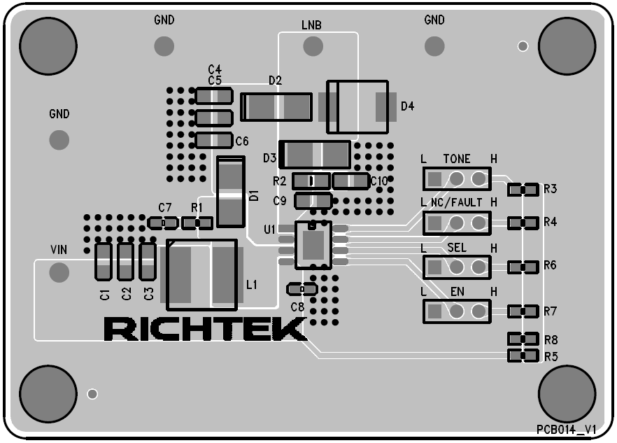
Top View
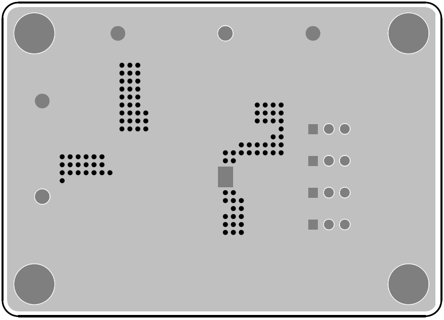
Bottom View