Richtek Designer Web Simulation Tool Technical Notes
Abstract
The Richtek Designer Web simulation tool allows the user to run accurate simulations of various popular Richtek parts. To get the best results from the tool in the shortest amount of time, this document provides some technical background information on the simulation models and calculation methods for various analysis options of the tool. It also explains some of the limitations of the tool, and gives advice for corrections to make sure your final application will match the simulated performance as closely as possible. Please note that the comments in this document mainly apply to the DC/DC converters which are included in the initial release of Richtek Designer.
1.
Introduction
The Richtek Designer Web simulation tool allows the user to run accurate simulations of various popular Richtek parts. To get the best results from the tool in the shortest amount of time, this document provides some technical background information on the simulation models and calculation methods for various analysis options of the tool. It also explains some of the limitations of the tool, and gives advice for corrections to make sure your final application will match the simulated performance as closely as possible. Please note that the comments in this document mainly apply to the DC/DC converters which are included in the initial release of Richtek Designer.
2.
Parts selection page
When making changes to parts selection filter values VIN / VOUT / IOUT , and the features and packages check boxes, the parts table will automatically change to match the user-selected values. The parts selected are based on the recommended values as listed in each IC’s datasheet.
Some explanation on certain feature options:
Continuous Operation Mode stands for parts that operate in constant frequency PWM mode without enhanced light load efficiency. The inductor current is continuous over the full load range. These parts are normally used in power supplies that need well-controlled operating frequency or that do not need special low power standby function.
Discontinuous Operation Mode stands for parts that will operate in a variable-frequency discontinuous mode when the inductor current reaches zero. At very light load operation, the switching frequency of these converters will be reduced to improve the light load efficiency. These parts are often used in supply rails that need to save power in low power standby modes.
OCP stands for Over Current Protection, typically a current limit function.
OVP stands for (output) Over Voltage Protection.
UVP stands for (output) Under Voltage Protection. OVP and UVP protection will become active when the output voltage exceeds certain levels (for example in output overload conditions). There are two kinds of OVP/UVP protections:
· Latch-Off Mode, which will latch the part when OVP/UVP is triggered
· Hiccup Mode, which will shut down the part when OVP/UVP is triggered, and later automatically restart the part.
Please see the device datasheet for more information.
3.
Design requirement page
After selecting a specific part, the menu will switch to the design requirements section. The default input voltage will be set with +/-20% tolerance, and can be adjusted by the user. The Vin Min and Vin Max can also be set to the same value. The steady state input voltage for analysis will be calculated from (VIN-max – VIN-min)/2 .
Output voltage and current can be set as well, and these will be the input for generating the application schematic component values.
Note that for buck converters, the input voltage must always be higher than the output voltage and one must also consider the converter max duty-cycle : 
(For ACOT devices, the max duty-cycle can be derived from the minimum OFF time and the switching frequency)
4.
Analyze page: Application schematic
Once the Create Design button is pressed, the simulation tool will automatically generate an application schematic.
Figure 1 below shows an example of a schematic generated for a DC/DC Buck converter part.
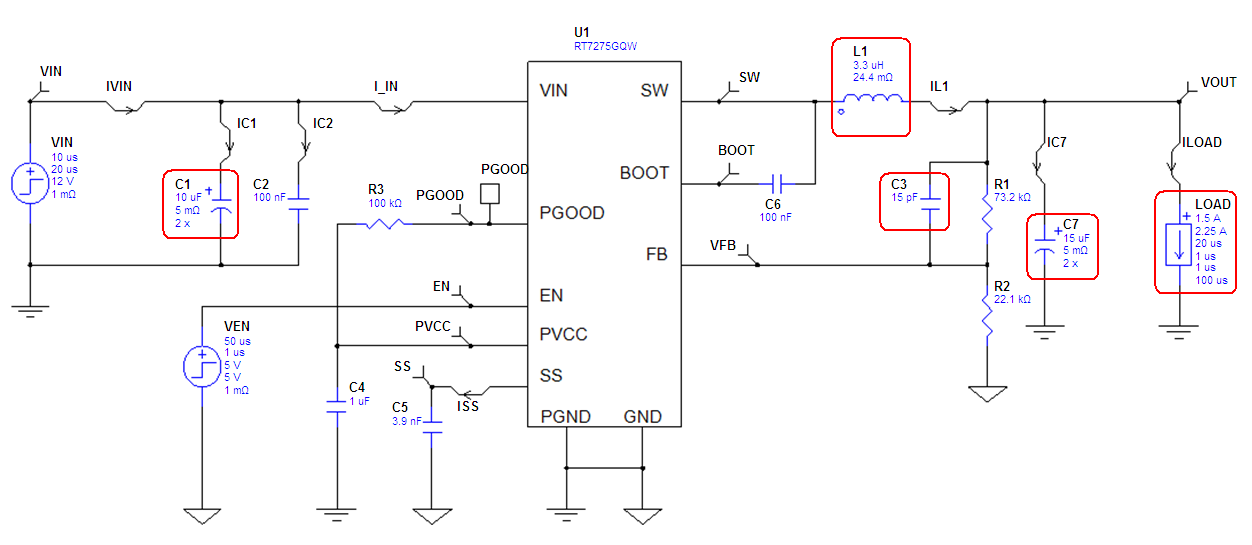
Figure 1: Automatically generated schematic with Keycomponents highlighted
The values of various key-components are based on certain design and performance aspects:
Default input voltage VIN is calculated from the average value of design requirements max and min values.
For checking load transients, the load component has a Start Current and a Pulse Current. The default start current is set at 50% of the Design Requirement max load value with step to a 75% pulse load current. The default load Rise Time and Fall Time are 1usec. These settings are quite suitable to check the converter general transient response.
To observe the closed loop damping, stability and output sag and soar effects, the rise and fall times may be reduced to 100 ~ 500nsec.
The default Inductor value L1 is calculated to achieve an inductor ripple of about 33% of the max load current condition.
Larger inductor values will decrease the ripple current, and subsequently reduce the output ripple voltage. Smaller inductor values will slightly improve load transient recovery speed.
The default output capacitor value C7 is calculated for 5% output voltage sag for an instantaneous full load transient from zero to I-max at the minimum input voltage.
 (see IC datasheet for more information)
Larger output capacitor values will improve sag and reduce output ripple. For parts with Discontinuous Operation Mode, a larger output capacitor may be needed to reduce the output ripple in light load operation.
For ACOT parts, larger output capacitors may also require an increase of the feed forward capacitor C3 for stable operation or good transient response.
For ACOT parts, the feed-forward capacitor C3 is normally needed for designs with output voltages higher than 1.5V and helps to damp the transient response. If it’s not needed, the software assigns it at a value of 1pF and it can be safely omitted. The default value will provide sufficiently damped response, but if you alter the impedance of the feedback network R1 / R2, adjust C3 to maintain a time constant between 250nsec ~ 350nsec. Also the C3 value should be increased when output capacitor C7 or inductor L1 is increased. The transient response simulation can be used to verify the correct value for C3: under-damped step response (ringing) means that C3 needs to be increased. When C3 is chosen too large, the output voltage will show a slow return to nominal value after the initial transient.
Input capacitor C1 default value is 2x10uF for output currents > 1.5A and 1x10uF for output currents <1.5A.
The input ripple and input capacitor RMS current can be verified via steady state simulation.
Input capacitor C2 is a small high frequency decoupling capacitor with very low ESR value. By setting the value to 1pF, one can see the effect that this capacitor has on input voltage rail high frequency noise.
5.
Steady-State analysis
In steady-state analysis, the circuit’s stable operation point is calculated at the nominal input voltage using the starting level of the load setting. The time scale is chosen to display around 5 switching cycles in PWM mode.
After each simulation, there are 5 different waveform sets available.
View Results shows an overview of these waveform sets:
Switching:
For viewing voltage and current waveforms related to the phase node. To check peak inductor current, RMS current in output capacitor, max voltage on the Bootstrap pin. Note that higher order effects like HF ringing due to parasitic inductances are not included. For ACOT models, the body diode conduction due to dead-time is not shown.
IC:
For viewing various voltage and current waveforms related to IC small signal pins.
VIN:
For examining input node voltages and currents: To check switching ripple on the input voltage rail, the RMS current in the input capacitors and the effect of HF decoupling capacitors.
OUTPUT:
For viewing the output switching ripple and load current.
ALL:
This window shows all waveforms, and allows you to choose specific waveforms to be shown together. It is most useful to see the relation between certain parameters that are not available from any of the above waveform sets.
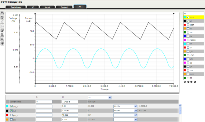
The below example shows how to examine waveforms in detail: Suppose we want to view the inductor current and output voltage ripple together in detail. To do this, follow these steps:
|
1. Select the Steady-State ALL waveform set
|
2. De-select all items using the x button, then select IL1 and VOUT by clicking their check boxes
|
|
|
|
|
3. As the voltage vertical scale is too large, zoom the voltage waveform to see the output switching ripple details
|
4. To bring the current waveform back to the display, click the vertical current scale, and change the unit to mA. The current waveform is now scaled back to original size.
|
|
|
|
|
|
Move an item to the top of the list by clicking on each one, then repeatedly clicking on the up arrows (^)
You can now select various measurements for IL1 and VOUT from the pull-down menu in the measurement section at the bottom.
|
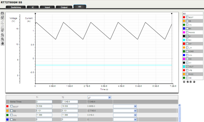
Output voltage accuracy check: The ACOT models in this simulation tool are quite accurate in many aspects. In ACOT voltage regulation, the FB voltage valley is compared to the internal reference, so the ripple on the FB pin has some influence on the output DC value. This simulation tool allows you to see this effect, and the influence of the feed-forward capacitor C3 on this behavior: Let’s run RT7275GQW in 3.3V output. To increase the output ripple, let’s choose a 2uH inductor and single 10uF capacitor. To exaggerate the effect of the feed forward capacitor, increase C3 to 33pF.
The feedback resistors are set for approximately 3.3V output voltage based on the normal calculation method  , with R1 and R2 selected from the standard 1% resistor values. In this example, the calculated nominal output voltage setting for the chosen resistor values would be:
  or 3.299V. See figure 2.
Figure 2
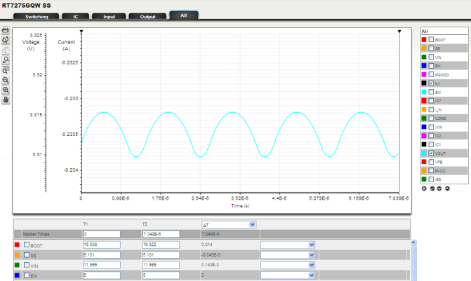
After running the steady-state simulation and examining the output waveform, you can see that the output peak to peak ripple is 33mV and the average output voltage value is 3.368V, so 69mV higher than the calculated 3.299V. See figure 3.
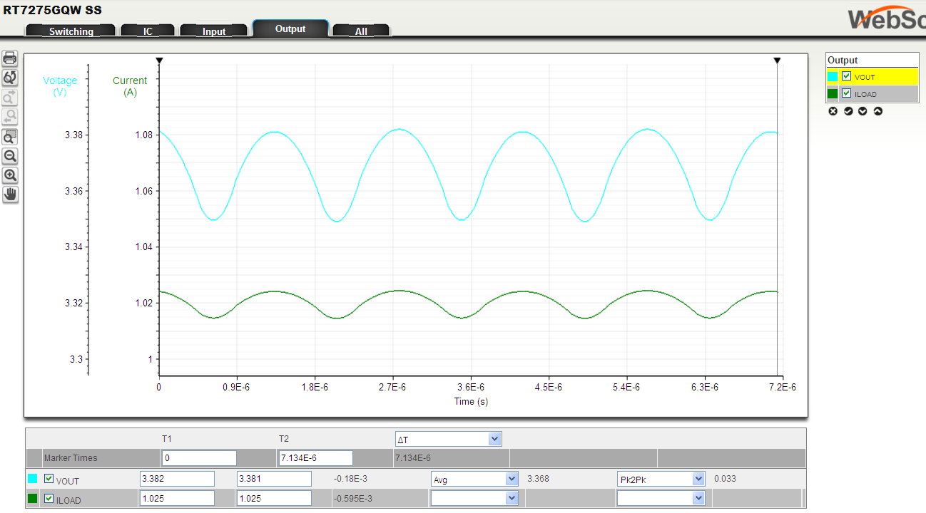
Figure 3
The explanation of the higher output voltage is that most of the 33mVpp output voltage ripple is transferred to the FB pin via feed-forward capacitor C3. Since the ACOT part regulates the FB voltage valley, the output voltage is therefore increased with a value determined by the difference between the average voltage and the valley voltage on the FB pin (around 20mV in this example), multiplied by the R1/R2 divider ratio. For applications where output voltage tolerances are very critical, the simulation tool can help to compensate for this effect.
6.
Transient analysis
In Transient simulation, the user can examine the circuit operation through changing load conditions. The simulation duration default is set at 0.2msec, but can be increased to as much as 5msec. Transient analysis can be used to check the circuit stability and output over- and undershoot. The model also includes the over-current and over-voltage protections, and protection behavior can be checked by increasing the load or even setting negative load conditions.
For parts that have Discontinuous Operation Mode at light load, the simulation duration in Steady-State analysis is too short to show much useful information. To examine the steady state operation for these parts in light load condition, it is better to run them in Transient Analysis with a longer simulation time. To modify the transient analysis into a longer steady-state condition, set the load start current and the pulse current values to the same level (ie 10mA for light load behavior).
After running the Transient Simulation, the same 5 waveform sets are available as described in the Steady State section. (SWITCHING, IC, VIN, OUTPUT, ALL)
Some example applications of the Transient Simulation are shown below:
1. In parts that have Discontinuous Operation Mode, it is sometimes good to know at what load current the part will switch from Discontinuous Mode to Continuous Mode. To check this, set the load start current at 10mA, pulse current at 1A, and increase the rise time to 5msec. Run the Transient simulation at 5msec time scale. Then select the ALL waveform window, de-select all waveforms and then select I-LOAD, I-L1 and VOUT. Zoom the VOUT scale as needed, and re-zoom the current scale my clicking the vertical current axis and changing the unit from A to mA. Figure 4 shows the simulation result for RT7276GQW 12V – 3.3V/2A application with a slowly increasing load. Use the cursor to select the area where the inductor current changes. The cursor readout will display the load where mode change occurs.
2.
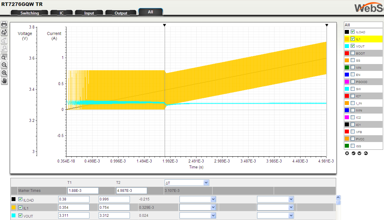
Figure 4: RT7276GQW with Gradual load increase shows where Discontinuous mode changes to Continuous Mode
3. Check ACOT converter stability
ACOT converters are stable over a wide range of input and output voltages and with different inductor and output capacitor values. However there are some cases where the system may show instable behavior:
a) when too small output capacitance is used, sub-harmonic oscillation can occur. (Please note that this only happens when very small output capacitor values are selected. In most applications, output capacitance is based on output ripple and transient response requirements, and the output capacitace values will not come near the low values that would lead to subharmonic instability. See the IC data sheet application section for more details).
b) when too large output capacitance is used in combination with higher output voltages, the control loop may become under-damped unless a sufficiently large C3 is used. (See also application note ACOT stability testing)
Let’s check an RT7240GSP 5V/4A ACOT application on stability: Select RT7240GSP on the Parts Selection page. On the Design Requirements page set the Operation Parameters to 12V input and 5V output, with a load current of 4A. Generate the schematic and increase the output capacitor from 2x22uF to 4x22uF. Change the Load current rise and fall times to 0.5usec. See the schematic in figure 5.
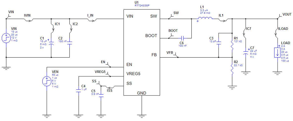
Figure 5: RT7240GSP in 12V to 5V / 4A supply with increased output capacitance.
When we now run the transient simulation, and select the output waveform set, it can be seen that the output voltage transient shows some ringing, indicating an under-damped response. See figure 6.
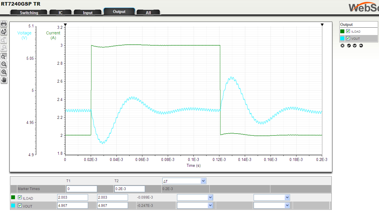
Figure 6: ACOT transient response with under-damped response.
The ACOT control loop damping can be improved by increasing the feed-forward capacitor C3. Figure 7 below shows the transient response with C3 increased from 12pF to 100pF, and the well damped response indicates that the circuit is stable.
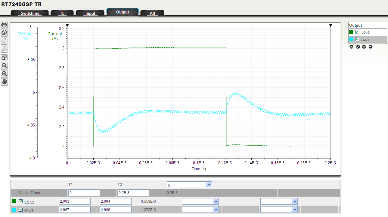
Figure 7: ACOT transient response with well damped response.
7.
Start-up analysis
In start-up analysis, the user can observe the circuit behavior in the startup phase when Input Voltage and Enable signals are applied. The simulation will accurately show the converter soft-start action, output voltage stabilization and PGOOD activation. The load level for start-up analysis will be the initial load setting (Start Current).
The Vin UVLO and Enable levels are accurately modeled, and the simulation results can be used for supply timing and power sequencing. The default time scale for Start-up analysis is 5msec, but can be increased to as much as 50msec. (Note that setting the simulation duration to 50msec will increase the simulation time considerably). The delay and rise time of both Vin and Enable can be set, to allow start-up from Vin or start-up from Enable.
Start-up from Enable:
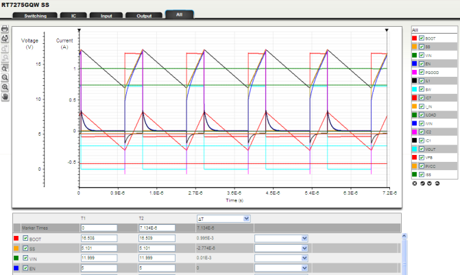
Figure 8 simulation below shows the start-up from the Enable signal for the RT7275GQW in a 3.3V application.
For this simulation, the Enable signal delay was set to 50usec and its rise time at 5msec. The Start-up analysis simulation stop time was set to 10msec.
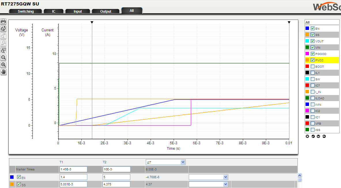
Figure 8: RT7275GQW start-up from Enable
To understand the start-up from EN, the following signals are shown: VIN, PVCC, EN, SS, VOUT, PGOOD.
When Vin goes to 12V, the converter operates in a low power standby mode. Then when EN slowly rises and passes the internal VCC start-up threshold (typically 0.7V), PVCC becomes active. EN rises further, and passes the converter lockout threshold (1.4V typically), the SS current source becomes active and charges the soft-start capacitor, and the SS voltage rises. When the SS voltage passes the 0.6V level, the converter starts to switch in discontinuous mode with small pulses, and Vin slowly rises, at the rate set by the SS voltage rise. The nominal VOUT voltage level is reached when SS reaches 1.36V. Even though Vout reaches its nominal value earlier, PGOOD rises when SS passes the 2.2V level, to allow some delay in PGOOD signaling.
Start-up from VIN:
Figure 9 below shows the start-up from VIN simulation of RT7275GQW in a 3.3V application.
For this simulation, the VIN signal delay was set to 50usec and its rise time at 5msec.
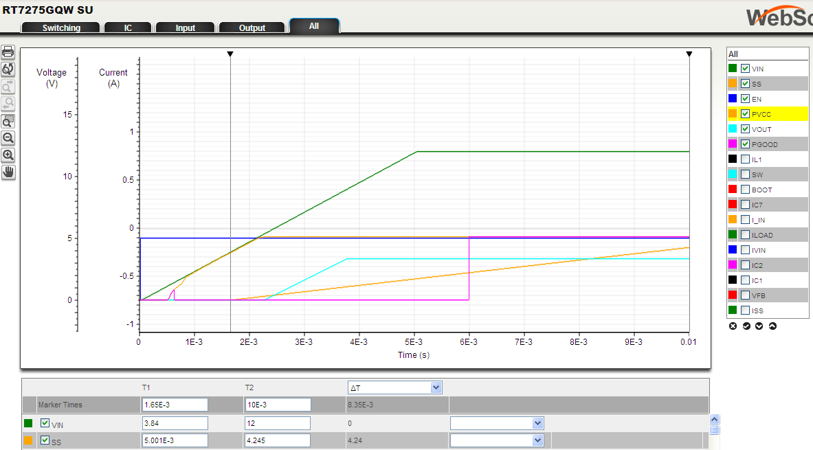
Figure 9: RT7275GQW start-up from VIN
To understand the start-up from VIN waveforms, the following signals are shown: VIN, PVCC, EN, SS, VOUT, PGOOD.
Simulation starts with EN high but VIN at zero. When VIN slowly rises, the internal PVCC LDO will become active and PVCC rises with VIN. When PVCC passes the UVLO threshold (3.85V typically), the SS current source becomes active and charges the soft-start capacitor, and the SS voltage rises. When SS voltage passes the 0.6V level, the converter starts to switch in discontinuous mode with small pulses, and Vin slowly rises with the rate set by the SS voltage rise. The nominal VOUT voltage level is reached when SS reaches 1.36V. PGOOD rises when SS passes the 2.2V level, to allow some delay in PGOOD signaling.
8.
Efficiency analysis
The efficiency analysis will provide information about the system total efficiency. The calculations are based on the components in the schematic diagram and include many detailed parameters like bias quiescent current losses, gate drive losses, MOSFET Rdson conduction losses, dead time losses, inductor DCR and core losses, and input and output capacitor ESR losses. Discontinuous mode parts will show the reduced losses in light load condition. Temperature effects on various parameters are included as well.
The efficiency is calculated based on  and is calculated for load currents from 1% to 100% of the pulse load current value as shown in the schematic.
Figure 10 shows the efficiency plot of RT7276GQW in a 12V to 3.3V / 2A application. By moving the mouse over the curve, the efficiency value at a specific load current will be shown.
RT7276GQW is a part with Discontinuous Operation Mode and the plot clearly shows the improved efficiency at light load condition below 0.3A load current.
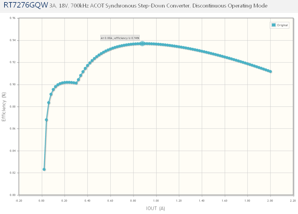
Figure 10: Efficiency of RT7276GQW in 12V to 3.3V / 2A application.
9.
BOM generation
When selecting the BOM tab, an automatic Bill of Material will be generated from the application schematic.
At the top BOM selection page, different distributors can be selected and components with pricing will be shown. Figure 11 below shows the default BOM generation for RT7276GW 12V to 3.3V / 2A application.
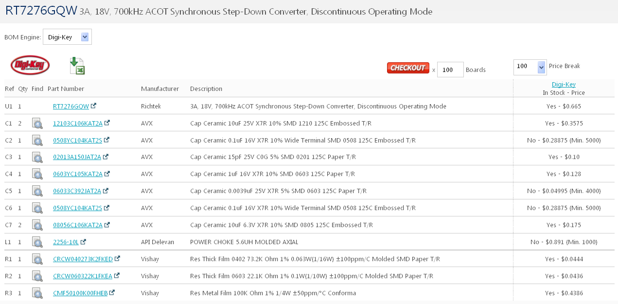
Figure 11: RT7276GQW 12V to 3.3V / 2A applicaTION default BOM
There are some limitations in the BOM generation engine. It is advisable to check the component selection in detail, to make sure they are appropriate:
Inductor type may need to be modified: normally SMD types are more suitable than leaded types.
Input and output capacitors need to be checked for dielectric type, rating and capacitance. This is especially important for the output capacitor in applications with higher output voltage, as the automatic BOM generation engine does not take the ceramic capacitor DC bias effect into account:
In the RT7276GQW 12V – 3.3V / 2A example above, the schematic shows output capacitance C7 as 2x10uF with 5mΩ ESR. All simulation calculations are based on these values.
In the BOM list, the default capacitor is an AVX 08056C106KAT2A 10uF/6.3V 0805 size ceramic capacitor. The AVX datasheet does not provide information on capacitance vs DC bias, but based on other suppliers data the actual capacitance of a standard 10uF/6.3V 0805 size MLCC at 3.3Vdc is around 20% lower than the rated value at zero bias voltage. At 5Vdc its value typically drops by 40%! To achieve the full simulated results in a real world circuit, compensate for this effect by using larger size capacitors or additional capacitors.
See figure 12 and 13: MLCC DC bias comparison between 0805 and 1206 size capacitors. (Murata datasheets)
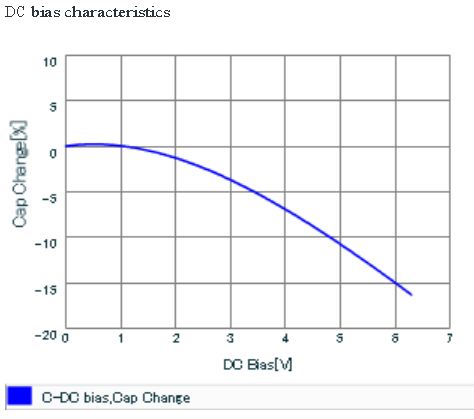
Figure 12: DC Bias effect of 10uF/6.3V 0805 size MLCC
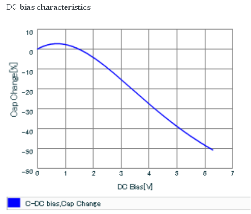
Figure 13: DC Bias effect of 10uF/6.3V 1206 size MLCC
In the final component selection, it is important to include these component variations, to avoid significant deviations between simulation results and the actual circuit operation.
10.
Summary section
The summary section will show a list of all performed simulations, efficiency data and final BOM selection. This summary can be printed, or saved as PDF.
It is also possible to save each design, so it can be accessed again at later stage.
11.
Summary
By means of the Richtek Designer Web Simulation tool the user is able to quickly generate an application schematic based on specific application requirements and Richtek device selection. The application can be verified on steady state, transient start-up sequence and efficiency, to check and verify that the circuit meets the end application requirements. A BOM list and summary can be generated. As with all simulation tools, the models have some limitations. Final verification by means of an IC evaluation board is highly recommended to ensure the design is suitable to be used in the end application.
In this first release of Richtek Designer, the models of the popular ACOT series are included. More models of popular Current Mode Buck will be released soon. Please check back regularly for updates.