8
8
8
4
1rem
1rem
1rem
1rem
rt-dark-800
headline-3
false
true
basicInfoTitle
12
12
12
12
left
buttonDownload
text-with-icon
secondary
i18n(button-item.download.button-label)
i18n(button-item.download.button-link)
_self


false
buttonContactUs
text-with-icon
secondary
i18n(button-item.contact-us.button-label)
i18n(button-item.contact-us.button-link)
_self


false
36
24
24
12
rt-dark-800
basicInfoSubtitle
basicInfoImageSwitcher
The RT9746 is an overvoltage protection devices feature a low 35mΩ (typ) RON internal FET with PTVS diode. The PTVS also protects the devices from surges up to 100V. When the input voltage exceeds the overvoltage threshold, the internal FET is turned off to prevent damage to the protected down stream components. The internal Over Voltage Thresholds (OVP) are preset to 6.8V typical. The RT9746 also feature an over-current protection and up to 4.5A. The RT9746 is offered in a small WL-CSP-12B (BSC) package provides small PCB area applications.
3
EVB_RT9746WSC
anchor
overviewSection
i18n(anchor-tab.overview-section.title)
overviewSectionAnchorTab
designResourceSection
i18n(anchor-tab.design-resource-section.title)
designResourceSectionAnchorTab
relatedProductSection
i18n(anchor-tab.related-product-section.title)
relatedProductSectionAnchorTab
orderingInformationSection
i18n(anchor-tab.ordering-information-section.title)
orderingInformationSectionAnchorTab
32
32
32
24
overview
1. Purpose
<p class="MsoNormal">The RT9746 is a VBUS OVP protector switch. This document explains the function and use of the RT9746 evaluation board (EVB), and provides information to enable operation, output voltage setting of the evaluation board.</p>
2. Introduction
<h3>General Product Information</h3> <p class="bady">The RT9746 is an over voltage protection devices feature a low 35mΩ (typ) RON internal FET with PTVS diode. The PTVS also protects the devices from surges up to 100V. When the input voltage exceeds the overvoltage threshold, the internal FET is turned off to prevent damage to the protected down stream components. The internal Over Voltage Thresholds (OVP) are preset to 6.8V typical. The RT9746 also feature an over-current protection and up to 4.5A. The RT9746 is offered in a small WL-CSP-12B (BSC) package provides small PCB area applications.</p> <h3><br /> Product Feature</h3> <ul> <li> PTVS Diode Embedded for VBUS Surge Protection </li> <li> Warning Indicator for OVP or UVP </li> <li> 28V Maximum Rating for DC Adapt </li> <li> Integrated Over-Voltage and Over Current Protection FET on VBUS for Fault Isolation </li> </ul> <h3><br /> Key Performance Summary Table</h3> <table class="MsoTableLightListAccent2" border="1" cellspacing="0" cellpadding="0" width="680" style="width:18.0cm;border-collapse:collapse;border:none"> <tr style="height:17.0pt"> <td width="34%" style="width:34.94%;border:solid #009EB8 1.0pt;background: #009EB8;padding:0cm 5.4pt 0cm 5.4pt;height:17.0pt"> <p class="ListParagraph1CxSpFirst">Key Features</p> </td> <td width="65%" style="width:65.06%;border:solid #009EB8 1.0pt;border-left: none;background:#009EB8;padding:0cm 5.4pt 0cm 5.4pt;height:17.0pt"> <p class="ListParagraph1CxSpLast">Evaluation Board Number: PCB083_V1</p> </td> </tr> <tr style="height:17.0pt"> <td width="34%" style="width:34.94%;border:solid #009EB8 1.0pt;border-top: none;padding:0cm 5.4pt 0cm 5.4pt;height:17.0pt"> <p class="ListParagraph1CxSpFirst">Default Input Voltage</p> </td> <td width="65%" style="width:65.06%;border-top:none;border-left:none; border-bottom:solid #009EB8 1.0pt;border-right:solid #009EB8 1.0pt; padding:0cm 5.4pt 0cm 5.4pt;height:17.0pt"> <p class="ListParagraph1CxSpLast">5V</p> </td> </tr> <tr style="height:17.0pt"> <td width="34%" style="width:34.94%;border:solid #009EB8 1.0pt;border-top: none;padding:0cm 5.4pt 0cm 5.4pt;height:17.0pt"> <p class="ListParagraph1CxSpFirst">Max Output Over Current</p> </td> <td width="65%" style="width:65.06%;border-top:none;border-left:none; border-bottom:solid #009EB8 1.0pt;border-right:solid #009EB8 1.0pt; padding:0cm 5.4pt 0cm 5.4pt;height:17.0pt"> <p class="ListParagraph1CxSpLast">4.5A</p> </td> </tr> <tr style="height:17.0pt"> <td width="34%" style="width:34.94%;border:solid #009EB8 1.0pt;border-top: none;padding:0cm 5.4pt 0cm 5.4pt;height:17.0pt"> <p class="ListParagraph1CxSpFirst">Default Marking & Package Type</p> </td> <td width="65%" style="width:65.06%;border-top:none;border-left:none; border-bottom:solid #009EB8 1.0pt;border-right:solid #009EB8 1.0pt; padding:0cm 5.4pt 0cm 5.4pt;height:17.0pt"> <p class="ListParagraph1CxSpLast">RT9746WSC, WL-CSP-12B 1.92x1.27 (BSC)</p> </td> </tr> </table>
3. Bench Test Setup Conditions
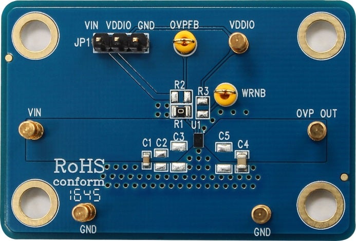
<p class="MsoNormal"><a class="fancybox" href="/content/dam/richtek-eds/resources/evaluation-boards/evb_rt9746wsc/html-images/image001_en.jpg"><img width="302" height="204" id="圖片 3" src="/content/dam/richtek-eds/resources/evaluation-boards/evb_rt9746wsc/html-images/image001_en.jpg" alt="Technical Document Image Preview" /></a></p> <p class="2">Carefully inspect all the components used in the EVB according to the following Bill of Materials table, and then make sure all the components are undamaged and correctly installed. If there is any missing or damaged component, which may occur during transportation, please contact our distributors or e-mail us at <a href="mailto:evb_service@richtek.com" class="link">evb_service@richtek.com</a>.</p> <h3><br /> Test Points</h3> <p class="MsoNormal">The EVB is provided with the test points and pin names listed in the table below.</p> <table class="MsoTableLightListAccent2" border="1" cellspacing="0" cellpadding="0" width="680" style="width:510.2pt;border-collapse:collapse;border:none"> <tr style="height:17.0pt"> <td width="12%" style="width:12.62%;border:solid #009EB8 1.0pt;background: #009EB8;padding:0cm 5.4pt 0cm 5.4pt;height:17.0pt"> <p class="23CxSpFirst">Test point/<br /> Pin name</p> </td> <td width="28%" style="width:28.68%;border:solid #009EB8 1.0pt;border-left: none;background:#009EB8;padding:0cm 5.4pt 0cm 5.4pt;height:17.0pt"> <p class="23CxSpMiddle">Signal</p> </td> <td width="58%" style="width:58.7%;border:solid #009EB8 1.0pt;border-left: none;background:#009EB8;padding:0cm 5.4pt 0cm 5.4pt;height:17.0pt"> <p class="23CxSpLast">Comment (expected waveforms or voltage levels on test points)</p> </td> </tr> <tr style="height:17.0pt"> <td width="12%" style="width:12.62%;border:solid #009EB8 1.0pt;border-top: none;padding:0cm 5.4pt 0cm 5.4pt;height:17.0pt"> <p class="ListParagraph1CxSpFirst">VIN</p> </td> <td width="28%" style="width:28.68%;border-top:none;border-left:none; border-bottom:solid #009EB8 1.0pt;border-right:solid #009EB8 1.0pt; padding:0cm 5.4pt 0cm 5.4pt;height:17.0pt"> <p class="ListParagraph1CxSpLast">Input voltage</p> </td> <td width="58%" style="width:58.7%;border-top:none;border-left:none; border-bottom:solid #009EB8 1.0pt;border-right:solid #009EB8 1.0pt; padding:0cm 5.4pt 0cm 5.4pt;height:17.0pt"> <p class="MsoNormal">VBUS from Power Adaptor.</p> </td> </tr> <tr style="height:17.0pt"> <td width="12%" style="width:12.62%;border:solid #009EB8 1.0pt;border-top: none;padding:0cm 5.4pt 0cm 5.4pt;height:17.0pt"> <p class="ListParagraph1">OVP OUT</p> </td> <td width="28%" style="width:28.68%;border-top:none;border-left:none; border-bottom:solid #009EB8 1.0pt;border-right:solid #009EB8 1.0pt; padding:0cm 5.4pt 0cm 5.4pt;height:17.0pt"> <p class="MsoNormal">Output voltage</p> </td> <td width="58%" style="width:58.7%;border-top:none;border-left:none; border-bottom:solid #009EB8 1.0pt;border-right:solid #009EB8 1.0pt; padding:0cm 5.4pt 0cm 5.4pt;height:17.0pt"> <p class="MsoNormal">Output from VBUS Load-Switch.</p> </td> </tr> <tr style="height:17.0pt"> <td width="12%" style="width:12.62%;border:solid #009EB8 1.0pt;border-top: none;padding:0cm 5.4pt 0cm 5.4pt;height:17.0pt"> <p class="ListParagraph1">OVPFB</p> </td> <td width="28%" style="width:28.68%;border-top:none;border-left:none; border-bottom:solid #009EB8 1.0pt;border-right:solid #009EB8 1.0pt; padding:0cm 5.4pt 0cm 5.4pt;height:17.0pt"> <p class="MsoNormal">External OVP Adjustment Setting</p> </td> <td width="58%" style="width:58.7%;border-top:none;border-left:none; border-bottom:solid #009EB8 1.0pt;border-right:solid #009EB8 1.0pt; padding:0cm 5.4pt 0cm 5.4pt;height:17.0pt"> <p class="MsoNormal">If no used, be surely tied to GND.</p> </td> </tr> <tr style="height:17.0pt"> <td width="12%" style="width:12.62%;border:solid #009EB8 1.0pt;border-top: none;padding:0cm 5.4pt 0cm 5.4pt;height:17.0pt"> <p class="ListParagraph1CxSpFirst">GND</p> </td> <td width="28%" style="width:28.68%;border-top:none;border-left:none; border-bottom:solid #009EB8 1.0pt;border-right:solid #009EB8 1.0pt; padding:0cm 5.4pt 0cm 5.4pt;height:17.0pt"> <p class="ListParagraph1CxSpMiddle">Ground</p> </td> <td width="58%" style="width:58.7%;border-top:none;border-left:none; border-bottom:solid #009EB8 1.0pt;border-right:solid #009EB8 1.0pt; padding:0cm 5.4pt 0cm 5.4pt;height:17.0pt"> <p class="ListParagraph1CxSpLast">Ground.</p> </td> </tr> <tr style="height:17.0pt"> <td width="12%" style="width:12.62%;border:solid #009EB8 1.0pt;border-top: none;padding:0cm 5.4pt 0cm 5.4pt;height:17.0pt"> <p class="ListParagraph1CxSpFirst">WRNB</p> </td> <td width="28%" style="width:28.68%;border-top:none;border-left:none; border-bottom:solid #009EB8 1.0pt;border-right:solid #009EB8 1.0pt; padding:0cm 5.4pt 0cm 5.4pt;height:17.0pt"> <p class="ListParagraph1CxSpMiddle">Inverse Warning Signal</p> </td> <td width="58%" style="width:58.7%;border-top:none;border-left:none; border-bottom:solid #009EB8 1.0pt;border-right:solid #009EB8 1.0pt; padding:0cm 5.4pt 0cm 5.4pt;height:17.0pt"> <p class="ListParagraph1CxSpLast">OCP,OTP, OVP, UVLO Flag Output (Open-Drain)</p> </td> </tr> </table> <h3><br /> Power-up</h3> <p class="MsoNormal">The RT9746 has a threshold of 2.7V power on reset (POR) with a built-in hysteresis of 100mV. Before the input voltage reaches the POR threshold, the RT9746 is off. When the input voltage is over the POR threshold, the VOUT of RT9746 will delay for 32ms which includes soft-start time of 8ms.</p> <h3>Input Over-Voltage Protection</h3> <p class="MsoNormal">The RT9746 provides input over-voltage protection via internal or external resistor to set OVP level. </p> <ul> <li> If OVPFB is connected to GND, the RT9746 uses the internal OVP level setting. </li> <li> If an external resistor-divider is connected to OVPFB and VOVPFB exceeds the VOVP_SEL voltage, the RT9746 will adopt external OVP level setting. The OVP level VOVP is set as below.<br /> <a class="fancybox" href="/content/dam/richtek-eds/resources/evaluation-boards/evb_rt9746wsc/html-images/image002_en.png"><img border="0" width="168" height="38" id="圖片 8" src="/content/dam/richtek-eds/resources/evaluation-boards/evb_rt9746wsc/html-images/image002_en.png" alt="Technical Document Image Preview" /></a> </li> </ul>
4. Schematic, Bill of Materials & Board Layout
<h3><br /> EVB Schematic Diagram</h3> <p class="a5"><a class="fancybox" href="/content/dam/richtek-eds/resources/evaluation-boards/evb_rt9746wsc/html-images/image003_en.png"><img border="0" width="669" height="305" id="圖片 5" src="/content/dam/richtek-eds/resources/evaluation-boards/evb_rt9746wsc/html-images/image003_en.png" alt="Technical Document Image Preview" /></a></p> <h3><br /> Bill of Materials</h3> <table class="MsoTableLightListAccent2" border="1" cellspacing="0" cellpadding="0" width="787" style="border-collapse:collapse;border:none"> <tr style="height:17.0pt"> <td width="11%" style="width:11.94%;border:solid #009EB8 1.0pt;background: #009EB8;padding:0cm 5.4pt 0cm 5.4pt;height:17.0pt"> <p class="MsoNormal">Reference</p> </td> <td width="5%" style="width:5.98%;border:solid #009EB8 1.0pt;border-left: none;background:#009EB8;padding:0cm 5.4pt 0cm 5.4pt;height:17.0pt"> <p class="MsoNormal">Qty</p> </td> <td width="23%" style="width:23.22%;border:solid #009EB8 1.0pt;border-left: none;background:#009EB8;padding:0cm 5.4pt 0cm 5.4pt;height:17.0pt"> <p class="MsoNormal">Part number</p> </td> <td width="19%" style="width:19.54%;border:solid #009EB8 1.0pt;border-left: none;background:#009EB8;padding:0cm 5.4pt 0cm 5.4pt;height:17.0pt"> <p class="MsoNormal">Description</p> </td> <td width="25%" style="width:25.66%;border:solid #009EB8 1.0pt;border-left: none;background:#009EB8;padding:0cm 5.4pt 0cm 5.4pt;height:17.0pt"> <p class="MsoNormal">Package</p> </td> <td width="13%" style="width:13.66%;border:solid #009EB8 1.0pt;border-left: none;background:#009EB8;padding:0cm 5.4pt 0cm 5.4pt;height:17.0pt"> <p class="MsoNormal">Manufacturer</p> </td> </tr> <tr style="height:1.0cm"> <td width="11%" style="width:11.94%;border:solid #009EB8 1.0pt;border-top: none;padding:0cm 5.4pt 0cm 5.4pt;height:1.0cm"> <p class="MsoNormal">U1</p> </td> <td width="5%" style="width:5.98%;border-top:none;border-left:none; border-bottom:solid #009EB8 1.0pt;border-right:solid #009EB8 1.0pt; padding:0cm 5.4pt 0cm 5.4pt;height:1.0cm"> <p class="MsoNormal">1</p> </td> <td width="23%" style="width:23.22%;border-top:none;border-left:none; border-bottom:solid #009EB8 1.0pt;border-right:solid #009EB8 1.0pt; padding:0cm 5.4pt 0cm 5.4pt;height:1.0cm"> <p class="MsoNormal">RT9746WSC</p> </td> <td width="19%" style="width:19.54%;border-top:none;border-left:none; border-bottom:solid #009EB8 1.0pt;border-right:solid #009EB8 1.0pt; padding:0cm 5.4pt 0cm 5.4pt;height:1.0cm"> <p class="MsoNormal">VBUS OVP IC with PTVS Diode</p> </td> <td width="25%" style="width:25.66%;border-top:none;border-left:none; border-bottom:solid #009EB8 1.0pt;border-right:solid #009EB8 1.0pt; padding:0cm 5.4pt 0cm 5.4pt;height:1.0cm"> <p class="MsoNormal">WL-CSP-12B 1.92x1.27(BSC)</p> </td> <td width="13%" style="width:13.66%;border-top:none;border-left:none; border-bottom:solid #009EB8 1.0pt;border-right:solid #009EB8 1.0pt; padding:0cm 5.4pt 0cm 5.4pt;height:1.0cm"> <p class="MsoNormal">RICHTEK</p> </td> </tr> <tr style="height:17.0pt"> <td width="11%" style="width:11.94%;border:solid #009EB8 1.0pt;border-top: none;padding:0cm 5.4pt 0cm 5.4pt;height:17.0pt"> <p class="MsoNormal">C1</p> </td> <td width="5%" style="width:5.98%;border-top:none;border-left:none; border-bottom:solid #009EB8 1.0pt;border-right:solid #009EB8 1.0pt; padding:0cm 5.4pt 0cm 5.4pt;height:17.0pt"> <p class="MsoNormal">1</p> </td> <td width="23%" style="width:23.22%;border-top:none;border-left:none; border-bottom:solid #009EB8 1.0pt;border-right:solid #009EB8 1.0pt; padding:0cm 5.4pt 0cm 5.4pt;height:17.0pt"> <p class="MsoNormal">C1608X7R1H104K080AA</p> </td> <td width="19%" style="width:19.54%;border-top:none;border-left:none; border-bottom:solid #009EB8 1.0pt;border-right:solid #009EB8 1.0pt; padding:0cm 5.4pt 0cm 5.4pt;height:17.0pt"> <p class="MsoNormal">0.1µF/50V/X7R/0603</p> </td> <td width="25%" style="width:25.66%;border-top:none;border-left:none; border-bottom:solid #009EB8 1.0pt;border-right:solid #009EB8 1.0pt; padding:0cm 5.4pt 0cm 5.4pt;height:17.0pt"> <p class="MsoNormal">C-0603</p> </td> <td width="13%" style="width:13.66%;border-top:none;border-left:none; border-bottom:solid #009EB8 1.0pt;border-right:solid #009EB8 1.0pt; padding:0cm 5.4pt 0cm 5.4pt;height:17.0pt"> <p class="MsoNormal">TDK</p> </td> </tr> <tr style="height:17.0pt"> <td width="11%" style="width:11.94%;border:solid #009EB8 1.0pt;border-top: none;padding:0cm 5.4pt 0cm 5.4pt;height:17.0pt"> <p class="MsoNormal">C4</p> </td> <td width="5%" style="width:5.98%;border-top:none;border-left:none; border-bottom:solid #009EB8 1.0pt;border-right:solid #009EB8 1.0pt; padding:0cm 5.4pt 0cm 5.4pt;height:17.0pt"> <p class="MsoNormal">1</p> </td> <td width="23%" style="width:23.22%;border-top:none;border-left:none; border-bottom:solid #009EB8 1.0pt;border-right:solid #009EB8 1.0pt; padding:0cm 5.4pt 0cm 5.4pt;height:17.0pt"> <p class="MsoNormal">C2012X7R1E105KT</p> </td> <td width="19%" style="width:19.54%;border-top:none;border-left:none; border-bottom:solid #009EB8 1.0pt;border-right:solid #009EB8 1.0pt; padding:0cm 5.4pt 0cm 5.4pt;height:17.0pt"> <p class="MsoNormal">1µF/25V/X7R/0805</p> </td> <td width="25%" style="width:25.66%;border-top:none;border-left:none; border-bottom:solid #009EB8 1.0pt;border-right:solid #009EB8 1.0pt; padding:0cm 5.4pt 0cm 5.4pt;height:17.0pt"> <p class="MsoNormal">C-0805</p> </td> <td width="13%" style="width:13.66%;border-top:none;border-left:none; border-bottom:solid #009EB8 1.0pt;border-right:solid #009EB8 1.0pt; padding:0cm 5.4pt 0cm 5.4pt;height:17.0pt"> <p class="MsoNormal">TDK</p> </td> </tr> <tr style="height:17.0pt"> <td width="11%" style="width:11.94%;border:solid #009EB8 1.0pt;border-top: none;padding:0cm 5.4pt 0cm 5.4pt;height:17.0pt"> <p class="MsoNormal">R1</p> </td> <td width="5%" style="width:5.98%;border-top:none;border-left:none; border-bottom:solid #009EB8 1.0pt;border-right:solid #009EB8 1.0pt; padding:0cm 5.4pt 0cm 5.4pt;height:17.0pt"> <p class="MsoNormal">1</p> </td> <td width="23%" style="width:23.22%;border-top:none;border-left:none; border-bottom:solid #009EB8 1.0pt;border-right:solid #009EB8 1.0pt; padding:0cm 5.4pt 0cm 5.4pt;height:17.0pt"> <p class="MsoNormal">0805T-5-0R</p> </td> <td width="19%" style="width:19.54%;border-top:none;border-left:none; border-bottom:solid #009EB8 1.0pt;border-right:solid #009EB8 1.0pt; padding:0cm 5.4pt 0cm 5.4pt;height:17.0pt"> <p class="MsoNormal">0R/0805</p> </td> <td width="25%" style="width:25.66%;border-top:none;border-left:none; border-bottom:solid #009EB8 1.0pt;border-right:solid #009EB8 1.0pt; padding:0cm 5.4pt 0cm 5.4pt;height:17.0pt"> <p class="MsoNormal">R-0805</p> </td> <td width="13%" style="width:13.66%;border-top:none;border-left:none; border-bottom:solid #009EB8 1.0pt;border-right:solid #009EB8 1.0pt; padding:0cm 5.4pt 0cm 5.4pt;height:17.0pt"> <p class="MsoNormal">RALEC</p> </td> </tr> </table> <h3><br /> PCB Layout</h3> <p class="23CxSpMiddle"><a class="fancybox" href="/content/dam/richtek-eds/resources/evaluation-boards/evb_rt9746wsc/html-images/image004_en.png"><img border="0" width="424" height="285" id="圖片 6" src="/content/dam/richtek-eds/resources/evaluation-boards/evb_rt9746wsc/html-images/image004_en.png" alt="Technical Document Image Preview" /></a></p> <p class="23CxSpLast">Top View</p> <p class="23CxSpFirst"><a class="fancybox" href="/content/dam/richtek-eds/resources/evaluation-boards/evb_rt9746wsc/html-images/image005_en.png"><img border="0" width="424" height="286" id="圖片 1" src="/content/dam/richtek-eds/resources/evaluation-boards/evb_rt9746wsc/html-images/image005_en.png" alt="Technical Document Image Preview" /></a></p> <p class="23CxSpLast">Bottom View</p>
32
32
32
0
design-resources
designResourceMultipleTable
56
32
32
32
24
24
24
24
i18n(tabs.related-product.title)
relatedProductTabs
i18n(tab-item.parameter-section.title)
parameterSection
parameterSectionTab
i18n(tab-item.package-size-pin-size-section.title)
packageSizePinsSizeSection
packageSizePinsSizeSectionTab
i18n(tab-item.product-feature-section.title)
productFeatureSection
productFeatureSectionTab
24
24
24
24
buttonSeeProductDifferences
text-with-icon
right
secondary-m
tertiary
i18n(button-item.see-product-differences.button-label)
i18n(button-item.see-product-differences.button-link)
_self


false
buttonFindOtherCategory
dropdown
i18n(button-item.find-other-category.button-label)
i18n(button-item.find-other-category.button-link)
_self
category-list
32
32
32
32
scrollable-table
parameterTable
normal-table
table-group
package-size-pins-size
packageSizePinsSizeTable
productFeature
24
24
24
24
i18n(tabs.ordering-information.title)
orderingInformationTabs
i18n(tab-item.evb-section.title)
evbSection
evbSectionTab
i18n(tab-item.product-section.title)
productSection
productSectionTab
24
24
24
24
evbImageSwitcher

normal-table
card-list
evb
evbTable
productImageSwitcher
normal-table
card-list
products
productTable