Selecting an Linear Regulator (LDO)
LDO Selection Criteria
In order to select a right LDO, some key criteria are important to be considered.
VIN (min)
| Is your input voltage able to drive the pass-element of LDO? |
|---|
|
VIN (max)
| Which upper bound of input voltage fits for your application best? |
|---|
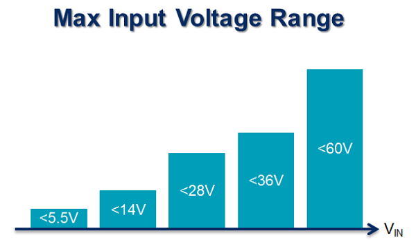
|
VOUT
IOUT
| What is the current requirement of your application? |
|---|
|
The current capability relates directly to dropout voltage and power dissipation. LDO controllers use external MOSFETs which can have larger current capability. 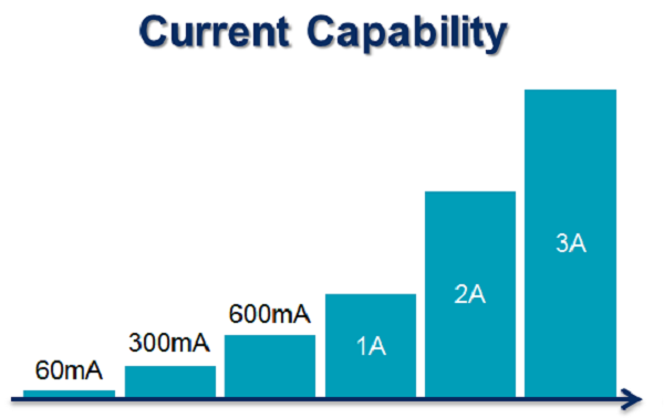
|
Power Dissipation
| How large is the power dissipation of your application? | |
|---|---|
|
The power dissipation in the LDO is determined by the voltage drop (VIN-VOUT) across the LDO multiplied by the current passing through the LDO (IOUT), which can be calculated from the formula PD = (VIN - VOUT) * ILOAD. The below graph shows the allowed LDO voltage drop versus LDO current for specific power dissipation values. 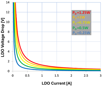
Larger current or larger voltage drop across the LDO quickly leads to high device power dissipation. The LDO package needs to be able to handle this power dissipation. Maximum allowed device power dissipation for SMD type LDOs depends on package, PCB layout and ambient temperature. You can calculate the allowed power dissipation by dividing the allowed temperature difference between junction and ambient by the thermal resistance between junction and ambient. The thermal resistance value θJA is shown in the datasheet, but keep in mind that this value is based on the JEDEC method, which can be slightly conservative. 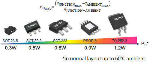
Here are some practical power dissipation limits for various package types, based on a normal PCB layout with some extra copper connected to the package pins and thermal pad, a maximum PCB ambient temperature of 60°C, and maximum silicon die temperature of 125°C. If your ambient temperature is lower, the power dissipation can be higher. If your PCB is small, or there are other hot components nearby, the maximum power dissipation may be less. Learn more about improving your thermal design in our tutorial video. 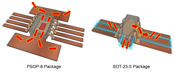
|
Duration : 5:00 (English, with user selectable subtitles) |
Dropout Voltage
| LDOs need a certain minimum voltage drop to regulate correctly. | |
|---|---|
|
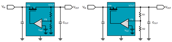
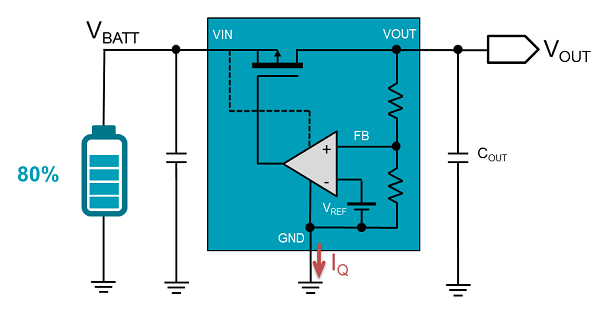
LDOs are Low Dropout Linear regulators. It basically means that these devices can still regulate the output voltage, even when the input voltage is very close to the output voltage. LDO dropout voltage is defined as the voltage drop across the regulator where the device can no longer regulate the output voltage. 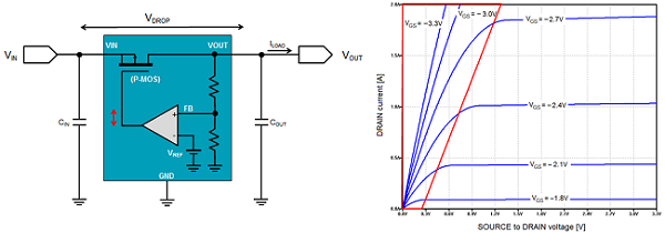
Here is the basic circuit of an LDO with a P-channel MOSFET pass device. The MOSFET source is connected to VIN. To regulate the output voltage, the error amplifier controls the P-MOSFET gate voltage with respect to VIN, thereby controlling the MOSFET conduction level. The LDO needs a certain amount of input to output voltage difference for regulation. When the difference between input and output voltage becomes smaller, the MOSFET operation shifts toward the MOSFET Ohmic region toward the left in the MOSFET I/V curves. In the Ohmic region, the MOSFET becomes resistive, and the error amplifier will pull the gate near ground level. At that point, the output voltage cannot be regulated anymore. 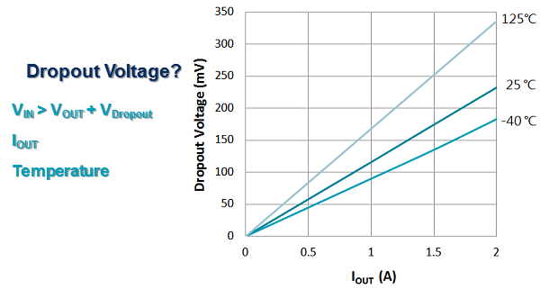
To maintain a well regulated LDO output voltage, you should make sure that the input voltage including ripple and tolerances is always higher than the output voltage + LDO dropout voltage. Dropout curves as shown in the LDO datasheet show this dropout voltage as a function of output current and temperature. These I/V curves basically represent the R DS(ON) of the pass MOSFET. Find out more LDO operation, dropout curves and a practical measurement example of the RT9187 dropout voltage vs. output current in our tutorial video. |
Duration : 3:13 (English, with user selectable subtitles) |
PSRR
| If your device is sensitive to supply ripple and noise, a low noise linear regulator is an ideal choice for this supply. | |
|---|---|
|
PSRR stands for power supply ripple rejection. The LDO PSRR value quantifies how well the LDO can reject input supply ripple at a certain frequency to keep the output voltage free of noise and ripple. In Richtek datasheets, PSRR is defined as the ripple attenuation ratio VOUT/VIN, therefore lower PSRR values are better. 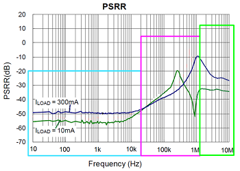
The diagram shows the example of PSRR vs. frequency. At frequencies up to 10kHz, LDOs have high open loop gain, and can reject input ripple very well. When frequency increases, the loop gain reduces due to the bandwidth limit of the LDO, and the PSRR curves rise. Higher LDO load pushes the load pole upwards, so the unity gain frequency at high load is also higher. In this example the LDO unity gain frequency is 300kHz at light load and 1MHz at high load, as can be seen from the peaks in the graph. Above the unity gain frequency, the LDO is not able to actively remove ripple. The ripple attenuation at these very high frequencies is mostly caused by the LDO output capacitor and the LDO internal parasitic impedance. Learn more about LDO PSRR and practical design tips for using a LDO as a ripple and noise filter in our tutorial video. 
|
Duration : 4:19 (English, with user selectable subtitles) |
Ultra Low Quiescent Current (IQ)
| Does your application need to run from a small battery cell for long periods? These applications often will run in sleep mode most of the time, and are only active for short periods. To minimize the power consumption in sleep mode, you need to select parts with very low quiescent current, and this is where Richtek ultra low IQ LDOs are really suitable. |
|
|---|---|
The LDO quiescent current is the current that is consumed by the IC internal feedback control and drive circuits. It is normally measured by measuring the current that flows out of the LDO ground pin. The Richtek Low IQ LDO portfolio contains LDOs with quiescent currents down to 1μA, which extends battery lifetime considerably. 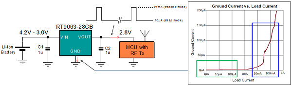
Richtek ultra low IQ LDOs provide dynamic quiescent current control for obtaining the best performance in battery powered applications requiring long battery life and good dynamic load performance. The Low IQ LDO RT9063 provides a stable 2.8V supply to the micro controller, and the LDO ground current stays relatively constant at 1μA in the low load range, thereby prolonging battery life. But at higher load currents, the ground current increases to improve the dynamic behavior of the LDO; when a sudden high load is encountered, the internal control circuit uses more energy to ensure a tight regulation of the output voltage. Find out more in our tutorial video. |
Duration : 3:15 (English, with user selectable subtitles) |