Selecting an Linear Regulator (LDO)
What is an LDO?
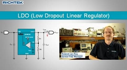
Find what Richtek can offer to accelerate your design time with this Richtek LDO Tutorial Video.
Duration : 5:27 (English, with user selectable subtitles)
Low-dropout (LDO) linear regulators are cost-effective and simple solutions for noise-sensitive applications where you need to drop a higher input voltage to a lower output voltage at relatively moderate power levels. They are especially suitable in applications which require low noise, low current and which have a small difference between the input and output voltage.
LDO Features
LDOs regulate the output voltage by controlling the conduction of the pass element in a linear regulation. This linear regulation provides accurate, noise free output voltage which can quickly respond to load changes on the output. The key advantage of an LDO is its simplicity and low cost design with low noise and fast voltage conversion.
However, compared to a switching regulator, an LDO has relatively low efficiency in applications with high VIN / VOUT ratio and power dissipation is more critical.
The linear regulation means that the voltage difference between input and output times the average load current is dissipated in the LDO pass element. Power Dissipation can be calculated as PD = (VIN - VOUT) * ILOAD, so big difference between VIN and VOUT with high load currents would lead to excessive dissipation.
Higher power dissipation requires LDOs in larger packages, which increases cost, PCB space and application heat. When LDO power dissipation exceeds ~ 0.8W, it is wise to look for alternatives like Buck converters.
Applications
When selecting an LDO, one should first consider the input and output voltage range, the LDO current capability and package dissipation capability. LDO dropout voltage is the minimum VIN - VOUT voltage where the device can regulate.
In micro power applications, (i.e. applications that need to run from a battery for several years) the LDO quiescent current IQ needs to be low to avoid unwanted battery drain,. These applications need special low IQ LDOs.
In applications that require a very clean and low noise output voltage, low noise and good PSRR will be the LDO key selection criteria.
LDO regulators are typically used when:
- converting a higher input voltage (VIN) into a lower output voltage (VOUT)
- a very clean power supply is required or when the application is noise sensitive
- the VIN/VOUT ratio is not very high, i.e. 3.3V to 2.5V
- the application draws moderate current (up to ~ 1A)
- The LDO power dissipation is limited, i.e. less than 0.8W
LDO Types
Below is simple explanation of LDO operation using two popular configurations based on pass element structures: LDOs with PMOS and NMOS pass elements.
PMOS-type LDO
For applications with VIN > 2.5V
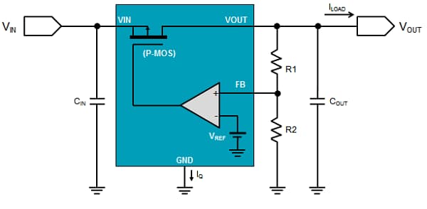
Here is the basic circuit of a PMOS LDO. It consists of a pass element Q1, a voltage reference and an error amplifier which controls the pass element. The error amplifier senses the output voltage via a resistor divider network.
In this drawing, the pass element is a P-channel MOSFET with the source connected to the input voltage.
The control loop is simple: The error amplifier controls the P-MOSFET gate to keep the voltage at the feedback pin at the same level as the voltage reference.
When the output voltage drops due to increased load or lower input voltage, the error amplifier lowers the gate voltage with respect to the source. This increases the conduction level of the P-MOSFET, and the output voltage rises again to the original regulated voltage.
In this configuration, the MOSFET can be controlled very close to the MOSFET ON level, which makes it possible to operate VIN very close to VOUT. But since the gate cannot be pulled lower than ground level, the input voltage must be high enough to allow sufficient headroom for the MOSFET gate-source voltage. To ensure sufficient MOSFET gate drive voltage, LDO's with P-MOSFET pass elements normally have a minimum input voltage requirement of around 2.5V.
NMOS-type LDO
(with external VBIAS or internal charge pump)
For applications with VIN > 1V
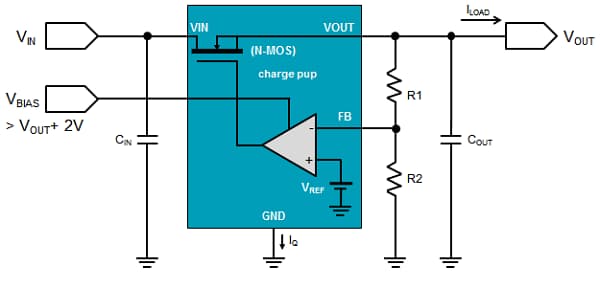
In some applications you may want to drive an LDO from a very low voltage supply rail. In these cases, you need to select an LDO with an N-channel MOSFET pass element.
LDO's with N-channel MOSFET pass elements need to provide a gate drive which is higher than the output voltage. In order to make it possible to use very low input and output voltages, many N-MOSFET LDO's have a gate drive circuit that is supplied by an internal charge-pump or external bias voltage. This makes it possible to use these LDOs with very low input voltages, down to 1V.
N-MOSFETs also have better RDS(ON) than similar sized P-MOSFETs, so their drop-out voltage is also lower, making it possible to supply more current in low voltage drop applications.
Below is an example of an NMOS LDO which provides a clean and stable 1.0V supply from a low 1.5V supply rail. Due to the low voltage drop of only 0.5V across the LDO, it can deliver more current without excessive dissipation.
