8
8
8
4
1rem
1rem
1rem
1rem
rt-dark-800
headline-3
false
true
basicInfoTitle
12
12
12
12
left
buttonDownload
text-with-icon
secondary
i18n(button-item.download.button-label)
i18n(button-item.download.button-link)
_self


false
buttonContactUs
text-with-icon
secondary
i18n(button-item.contact-us.button-label)
i18n(button-item.contact-us.button-link)
_self


false
36
24
24
12
rt-dark-800
basicInfoSubtitle
basicInfoImageSwitcher
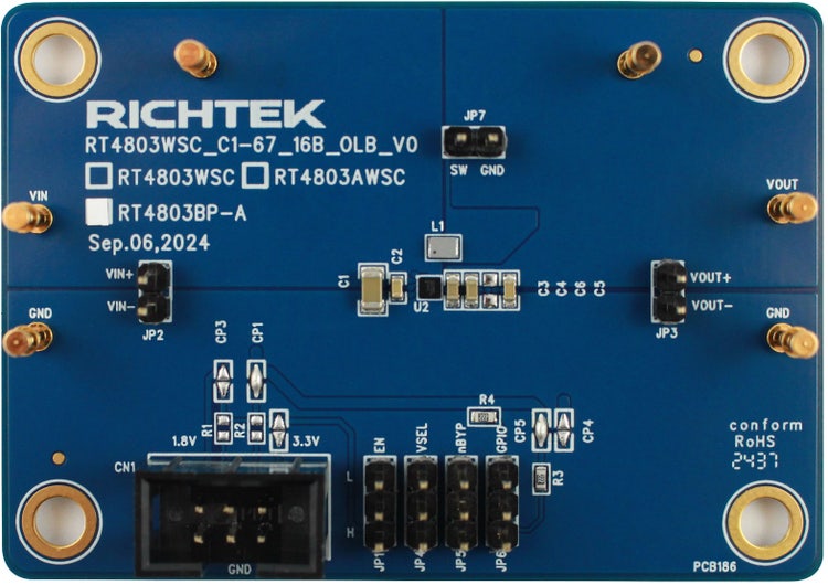
RT4803B 可帮助系统充分利用新一代电池化学技术,即使电池电压低于系统电源 IC 所需电压,仍可提供充足的能量。通过集成内置功率晶体管、同步整流及低供电电流等特性,RT4803B 为采用先进锂离子电池化学技术的系统提供紧凑且高效率的解决方案。 RT4803B 为升压稳压器,专为单节锂离子电池设计,即使电池电压低于系统所需的最低工作电压,仍可提供稳定的输出电压。在升压模式下,最高可支持 2000mA 负载电流,并保持输出电压稳定。关断模式下的静态电流低于 1μA,可有效延长电池使用寿命。该器件可在旁路模式与正常升压模式之间平滑切换,也可强制进入旁路模式,以进一步降低静态电流。
3
EVB_RT4803BP-A
anchor
overviewSection
i18n(anchor-tab.overview-section.title)
overviewSectionAnchorTab
designResourceSection
i18n(anchor-tab.design-resource-section.title)
designResourceSectionAnchorTab
relatedProductSection
i18n(anchor-tab.related-product-section.title)
relatedProductSectionAnchorTab
orderingInformationSection
i18n(anchor-tab.ordering-information-section.title)
orderingInformationSectionAnchorTab
32
32
32
24
overview
1. General Description
<p class="bady">The RT4803B allows systems to take advantage of new battery chemistries that can supply significant energy when the battery voltage is lower than the required voltage for system power ICs. By combining built-in power transistors, synchronous rectification, and low supply current, this IC provides a compact solution for systems using advanced Li-Ion battery chemistries.</p> <p class="bady">The RT4803B is a boost regulator designed to provide a minimum output voltage from a single-cell Li-Ion battery, even when the battery voltage is below the system minimum. In boost mode, output voltage regulation is guaranteed up to a maximum load current of 2000mA. The quiescent current in shutdown mode is less than 1µA, which maximizes battery life. The regulator transitions smoothly between bypass and normal boost modes. The device can be forced into bypass mode to reduce quiescent current.</p>
2. Performance Specification Summary
<p class="bady">Summary of the RT4803B Evaluation Board performance specificiaiton is provided in Table 1. The ambient temperature is 25°C.</p> <p class="MsoNormal">Table 1. RT4803B Evaluation Board Performance Specification Summary</p> <div> <table class="MsoTableLightListAccent2" border="1" cellspacing="0" cellpadding="0" width="680" style="border-collapse:collapse;border:none"> <tr style="height:17.0pt"> <td width="263" style="width:197.35pt;border:solid #009EB8 1.0pt;background: #009EB8;padding:0cm 5.4pt 0cm 5.4pt;height:17.0pt"> <p class="ListParagraph1CxSpFirst">Specification</p> </td> <td width="245" style="width:183.85pt;border:solid #009EB8 1.0pt;border-left: none;background:#009EB8;padding:0cm 5.4pt 0cm 5.4pt;height:17.0pt"> <p class="ListParagraph1CxSpMiddle">Test Conditions</p> </td> <td width="43" style="width:32.5pt;border:solid #009EB8 1.0pt;border-left:none; background:#009EB8;padding:0cm 5.4pt 0cm 5.4pt;height:17.0pt"> <p class="ListParagraph1CxSpMiddle">Min</p> </td> <td width="43" style="width:32.55pt;border:solid #009EB8 1.0pt;border-left: none;background:#009EB8;padding:0cm 5.4pt 0cm 5.4pt;height:17.0pt"> <p class="ListParagraph1CxSpMiddle">Typ</p> </td> <td width="43" style="width:32.55pt;border:solid #009EB8 1.0pt;border-left: none;background:#009EB8;padding:0cm 5.4pt 0cm 5.4pt;height:17.0pt"> <p class="ListParagraph1CxSpMiddle">Max</p> </td> <td width="42" style="width:31.4pt;border:solid #009EB8 1.0pt;border-left:none; background:#009EB8;padding:0cm 5.4pt 0cm 5.4pt;height:17.0pt"> <p class="ListParagraph1CxSpLast">Unit</p> </td> </tr> <tr style="height:17.0pt"> <td width="263" style="width:197.35pt;border:solid #009EB8 1.0pt;border-top: none;padding:0cm 5.4pt 0cm 5.4pt;height:17.0pt"> <p class="ListParagraph1CxSpFirst">Input Voltage Range</p> </td> <td width="245" style="width:183.85pt;border-top:none;border-left:none; border-bottom:solid #009EB8 1.0pt;border-right:solid #009EB8 1.0pt; padding:0cm 5.4pt 0cm 5.4pt;height:17.0pt"> </td> <td width="43" style="width:32.5pt;border-top:none;border-left:none;border-bottom: solid #009EB8 1.0pt;border-right:solid #009EB8 1.0pt;padding:0cm 5.4pt 0cm 5.4pt; height:17.0pt"> <p class="ListParagraph1CxSpMiddle">1.8</p> </td> <td width="43" style="width:32.55pt;border-top:none;border-left:none; border-bottom:solid #009EB8 1.0pt;border-right:solid #009EB8 1.0pt; padding:0cm 5.4pt 0cm 5.4pt;height:17.0pt"> <p class="ListParagraph1CxSpMiddle">--</p> </td> <td width="43" style="width:32.55pt;border-top:none;border-left:none; border-bottom:solid #009EB8 1.0pt;border-right:solid #009EB8 1.0pt; padding:0cm 5.4pt 0cm 5.4pt;height:17.0pt"> <p class="ListParagraph1CxSpMiddle">5</p> </td> <td width="42" style="width:31.4pt;border-top:none;border-left:none;border-bottom: solid #009EB8 1.0pt;border-right:solid #009EB8 1.0pt;padding:0cm 5.4pt 0cm 5.4pt; height:17.0pt"> <p class="ListParagraph1CxSpLast">V</p> </td> </tr> <tr style="height:17.0pt"> <td width="263" style="width:197.35pt;border:solid #009EB8 1.0pt;border-top: none;padding:0cm 5.4pt 0cm 5.4pt;height:17.0pt"> <p class="ListParagraph1CxSpFirst">Output Voltage Range</p> </td> <td width="245" style="width:183.85pt;border-top:none;border-left:none; border-bottom:solid #009EB8 1.0pt;border-right:solid #009EB8 1.0pt; padding:0cm 5.4pt 0cm 5.4pt;height:17.0pt"> </td> <td width="43" style="width:32.5pt;border-top:none;border-left:none;border-bottom: solid #009EB8 1.0pt;border-right:solid #009EB8 1.0pt;padding:0cm 5.4pt 0cm 5.4pt; height:17.0pt"> <p class="ListParagraph1CxSpMiddle">2.85</p> </td> <td width="43" style="width:32.55pt;border-top:none;border-left:none; border-bottom:solid #009EB8 1.0pt;border-right:solid #009EB8 1.0pt; padding:0cm 5.4pt 0cm 5.4pt;height:17.0pt"> <p class="ListParagraph1CxSpMiddle">--</p> </td> <td width="43" style="width:32.55pt;border-top:none;border-left:none; border-bottom:solid #009EB8 1.0pt;border-right:solid #009EB8 1.0pt; padding:0cm 5.4pt 0cm 5.4pt;height:17.0pt"> <p class="ListParagraph1CxSpMiddle">4.4</p> </td> <td width="42" style="width:31.4pt;border-top:none;border-left:none;border-bottom: solid #009EB8 1.0pt;border-right:solid #009EB8 1.0pt;padding:0cm 5.4pt 0cm 5.4pt; height:17.0pt"> <p class="ListParagraph1CxSpLast">V</p> </td> </tr> <tr style="height:1.0cm"> <td width="263" style="width:197.35pt;border:solid #009EB8 1.0pt;border-top: none;padding:0cm 5.4pt 0cm 5.4pt;height:1.0cm"> <p class="Default">Quiescent Current </p> </td> <td width="245" style="width:183.85pt;border-top:none;border-left:none; border-bottom:solid #009EB8 1.0pt;border-right:solid #009EB8 1.0pt; padding:0cm 5.4pt 0cm 5.4pt;height:1.0cm"> <p class="ListParagraph1CxSpFirst">Boost mode, I<sub>LOAD</sub> = 0mA, switching, V<sub>IN</sub> = 3V </p> </td> <td width="43" style="width:32.5pt;border-top:none;border-left:none;border-bottom: solid #009EB8 1.0pt;border-right:solid #009EB8 1.0pt;padding:0cm 5.4pt 0cm 5.4pt; height:1.0cm"> <p class="ListParagraph1CxSpMiddle">--</p> </td> <td width="43" style="width:32.55pt;border-top:none;border-left:none; border-bottom:solid #009EB8 1.0pt;border-right:solid #009EB8 1.0pt; padding:0cm 5.4pt 0cm 5.4pt;height:1.0cm"> <p class="ListParagraph1CxSpMiddle">56</p> </td> <td width="43" style="width:32.55pt;border-top:none;border-left:none; border-bottom:solid #009EB8 1.0pt;border-right:solid #009EB8 1.0pt; padding:0cm 5.4pt 0cm 5.4pt;height:1.0cm"> <p class="ListParagraph1CxSpMiddle">100</p> </td> <td width="42" style="width:31.4pt;border-top:none;border-left:none;border-bottom: solid #009EB8 1.0pt;border-right:solid #009EB8 1.0pt;padding:0cm 5.4pt 0cm 5.4pt; height:1.0cm"> <p class="ListParagraph1CxSpLast">µA</p> </td> </tr> <tr style="height:17.0pt"> <td width="263" style="width:197.35pt;border:solid #009EB8 1.0pt;border-top: none;padding:0cm 5.4pt 0cm 5.4pt;height:17.0pt"> <p class="ListParagraph1CxSpFirst">Shutdown Current</p> </td> <td width="245" style="width:183.85pt;border-top:none;border-left:none; border-bottom:solid #009EB8 1.0pt;border-right:solid #009EB8 1.0pt; padding:0cm 5.4pt 0cm 5.4pt;height:17.0pt"> </td> <td width="43" style="width:32.5pt;border-top:none;border-left:none;border-bottom: solid #009EB8 1.0pt;border-right:solid #009EB8 1.0pt;padding:0cm 5.4pt 0cm 5.4pt; height:17.0pt"> <p class="ListParagraph1CxSpMiddle">--</p> </td> <td width="43" style="width:32.55pt;border-top:none;border-left:none; border-bottom:solid #009EB8 1.0pt;border-right:solid #009EB8 1.0pt; padding:0cm 5.4pt 0cm 5.4pt;height:17.0pt"> <p class="ListParagraph1CxSpMiddle">--</p> </td> <td width="43" style="width:32.55pt;border-top:none;border-left:none; border-bottom:solid #009EB8 1.0pt;border-right:solid #009EB8 1.0pt; padding:0cm 5.4pt 0cm 5.4pt;height:17.0pt"> <p class="ListParagraph1CxSpMiddle">2</p> </td> <td width="42" style="width:31.4pt;border-top:none;border-left:none;border-bottom: solid #009EB8 1.0pt;border-right:solid #009EB8 1.0pt;padding:0cm 5.4pt 0cm 5.4pt; height:17.0pt"> <p class="ListParagraph1CxSpLast">µA</p> </td> </tr> <tr style="height:17.0pt"> <td width="263" style="width:197.35pt;border:solid #009EB8 1.0pt;border-top: none;padding:0cm 5.4pt 0cm 5.4pt;height:17.0pt"> <p class="ListParagraph1CxSpFirst">Output Voltage Accuracy </p> </td> <td width="245" style="width:183.85pt;border-top:none;border-left:none; border-bottom:solid #009EB8 1.0pt;border-right:solid #009EB8 1.0pt; padding:0cm 5.4pt 0cm 5.4pt;height:17.0pt"> <p class="ListParagraph1CxSpMiddle">V<sub>OUT</sub> - V<sub>IN</sub> > 100mV, PWM </p> </td> <td width="43" style="width:32.5pt;border-top:none;border-left:none;border-bottom: solid #009EB8 1.0pt;border-right:solid #009EB8 1.0pt;padding:0cm 5.4pt 0cm 5.4pt; height:17.0pt"> <p class="ListParagraph1CxSpMiddle"><span lang="EN-US" style="font-size:10.0pt;font-family:Symbol">-</span>2</p> </td> <td width="43" style="width:32.55pt;border-top:none;border-left:none; border-bottom:solid #009EB8 1.0pt;border-right:solid #009EB8 1.0pt; padding:0cm 5.4pt 0cm 5.4pt;height:17.0pt"> <p class="ListParagraph1CxSpMiddle">--</p> </td> <td width="43" style="width:32.55pt;border-top:none;border-left:none; border-bottom:solid #009EB8 1.0pt;border-right:solid #009EB8 1.0pt; padding:0cm 5.4pt 0cm 5.4pt;height:17.0pt"> <p class="ListParagraph1CxSpMiddle">2</p> </td> <td width="42" style="width:31.4pt;border-top:none;border-left:none;border-bottom: solid #009EB8 1.0pt;border-right:solid #009EB8 1.0pt;padding:0cm 5.4pt 0cm 5.4pt; height:17.0pt"> <p class="ListParagraph1CxSpLast">%</p> </td> </tr> <tr style="height:17.0pt"> <td width="263" style="width:197.35pt;border:solid #009EB8 1.0pt;border-top: none;padding:0cm 5.4pt 0cm 5.4pt;height:17.0pt"> <p class="ListParagraph1CxSpFirst">Boost Valley Current Limit</p> </td> <td width="245" style="width:183.85pt;border-top:none;border-left:none; border-bottom:solid #009EB8 1.0pt;border-right:solid #009EB8 1.0pt; padding:0cm 5.4pt 0cm 5.4pt;height:17.0pt"> <p class="ListParagraph1CxSpMiddle">V<sub>IN</sub> = 2.9V </p> </td> <td width="43" style="width:32.5pt;border-top:none;border-left:none;border-bottom: solid #009EB8 1.0pt;border-right:solid #009EB8 1.0pt;padding:0cm 5.4pt 0cm 5.4pt; height:17.0pt"> <p class="ListParagraph1CxSpMiddle">3.5</p> </td> <td width="43" style="width:32.55pt;border-top:none;border-left:none; border-bottom:solid #009EB8 1.0pt;border-right:solid #009EB8 1.0pt; padding:0cm 5.4pt 0cm 5.4pt;height:17.0pt"> <p class="ListParagraph1CxSpMiddle">4</p> </td> <td width="43" style="width:32.55pt;border-top:none;border-left:none; border-bottom:solid #009EB8 1.0pt;border-right:solid #009EB8 1.0pt; padding:0cm 5.4pt 0cm 5.4pt;height:17.0pt"> <p class="ListParagraph1CxSpMiddle">4.5</p> </td> <td width="42" style="width:31.4pt;border-top:none;border-left:none;border-bottom: solid #009EB8 1.0pt;border-right:solid #009EB8 1.0pt;padding:0cm 5.4pt 0cm 5.4pt; height:17.0pt"> <p class="ListParagraph1CxSpLast">A</p> </td> </tr> <tr style="height:1.0cm"> <td width="263" style="width:197.35pt;border:solid #009EB8 1.0pt;border-top: none;padding:0cm 5.4pt 0cm 5.4pt;height:1.0cm"> <p class="ListParagraph1CxSpFirst">Operation Frequency</p> </td> <td width="245" style="width:183.85pt;border-top:none;border-left:none; border-bottom:solid #009EB8 1.0pt;border-right:solid #009EB8 1.0pt; padding:0cm 5.4pt 0cm 5.4pt;height:1.0cm"> <p class="ListParagraph1CxSpMiddle">V<sub>IN</sub> = 2.65V, V<sub>OUT</sub> = 3.5V, I<sub>LOAD</sub> = 1000mA </p> </td> <td width="43" style="width:32.5pt;border-top:none;border-left:none;border-bottom: solid #009EB8 1.0pt;border-right:solid #009EB8 1.0pt;padding:0cm 5.4pt 0cm 5.4pt; height:1.0cm"> <p class="ListParagraph1CxSpMiddle">--</p> </td> <td width="43" style="width:32.55pt;border-top:none;border-left:none; border-bottom:solid #009EB8 1.0pt;border-right:solid #009EB8 1.0pt; padding:0cm 5.4pt 0cm 5.4pt;height:1.0cm"> <p class="ListParagraph1CxSpMiddle">2.5</p> </td> <td width="43" style="width:32.55pt;border-top:none;border-left:none; border-bottom:solid #009EB8 1.0pt;border-right:solid #009EB8 1.0pt; padding:0cm 5.4pt 0cm 5.4pt;height:1.0cm"> <p class="ListParagraph1CxSpMiddle">--</p> </td> <td width="42" style="width:31.4pt;border-top:none;border-left:none;border-bottom: solid #009EB8 1.0pt;border-right:solid #009EB8 1.0pt;padding:0cm 5.4pt 0cm 5.4pt; height:1.0cm"> <p class="ListParagraph1CxSpLast">MHz</p> </td> </tr> <tr style="height:1.0cm"> <td width="263" style="width:197.35pt;border:solid #009EB8 1.0pt;border-top: none;padding:0cm 5.4pt 0cm 5.4pt;height:1.0cm"> <p class="ListParagraph1">SCL, SDA High-Level Input Threshold Voltage </p> </td> <td width="245" style="width:183.85pt;border-top:none;border-left:none; border-bottom:solid #009EB8 1.0pt;border-right:solid #009EB8 1.0pt; padding:0cm 5.4pt 0cm 5.4pt;height:1.0cm"> </td> <td width="43" style="width:32.5pt;border-top:none;border-left:none;border-bottom: solid #009EB8 1.0pt;border-right:solid #009EB8 1.0pt;padding:0cm 5.4pt 0cm 5.4pt; height:1.0cm"> <p class="Default">0.84 </p> </td> <td width="43" style="width:32.55pt;border-top:none;border-left:none; border-bottom:solid #009EB8 1.0pt;border-right:solid #009EB8 1.0pt; padding:0cm 5.4pt 0cm 5.4pt;height:1.0cm"> <p class="ListParagraph1CxSpFirst">--</p> </td> <td width="43" style="width:32.55pt;border-top:none;border-left:none; border-bottom:solid #009EB8 1.0pt;border-right:solid #009EB8 1.0pt; padding:0cm 5.4pt 0cm 5.4pt;height:1.0cm"> <p class="ListParagraph1CxSpMiddle">--</p> </td> <td width="42" style="width:31.4pt;border-top:none;border-left:none;border-bottom: solid #009EB8 1.0pt;border-right:solid #009EB8 1.0pt;padding:0cm 5.4pt 0cm 5.4pt; height:1.0cm"> <p class="ListParagraph1CxSpLast">V</p> </td> </tr> <tr style="height:1.0cm"> <td width="263" style="width:197.35pt;border:solid #009EB8 1.0pt;border-top: none;padding:0cm 5.4pt 0cm 5.4pt;height:1.0cm"> <p class="ListParagraph1">SCL, SDA Low-Level Input Threshold Voltage </p> </td> <td width="245" style="width:183.85pt;border-top:none;border-left:none; border-bottom:solid #009EB8 1.0pt;border-right:solid #009EB8 1.0pt; padding:0cm 5.4pt 0cm 5.4pt;height:1.0cm"> </td> <td width="43" style="width:32.5pt;border-top:none;border-left:none;border-bottom: solid #009EB8 1.0pt;border-right:solid #009EB8 1.0pt;padding:0cm 5.4pt 0cm 5.4pt; height:1.0cm"> <p class="ListParagraph1CxSpFirst">--</p> </td> <td width="43" style="width:32.55pt;border-top:none;border-left:none; border-bottom:solid #009EB8 1.0pt;border-right:solid #009EB8 1.0pt; padding:0cm 5.4pt 0cm 5.4pt;height:1.0cm"> <p class="ListParagraph1CxSpLast">--</p> </td> <td width="43" style="width:32.55pt;border-top:none;border-left:none; border-bottom:solid #009EB8 1.0pt;border-right:solid #009EB8 1.0pt; padding:0cm 5.4pt 0cm 5.4pt;height:1.0cm"> <p class="Default">0.36</p> </td> <td width="42" style="width:31.4pt;border-top:none;border-left:none;border-bottom: solid #009EB8 1.0pt;border-right:solid #009EB8 1.0pt;padding:0cm 5.4pt 0cm 5.4pt; height:1.0cm"> <p class="ListParagraph1">V</p> </td> </tr> </table> </div>
3. Power-up Procedure
<h3>Suggestion Required Equipments</h3> <ul> <li>RT4803B Evaluation Board </li> <li>DC power supply capable</li> <li>Electronic load</li> </ul>
4. Quick Start Procedures
<p class="bady">The Evaluation Board is fully assembled and tested. Follow the steps below to verify board operation. Do not turn on supplies until all connections are made. When measuring the output voltage ripple, care must be taken to avoid a long ground lead on the oscilloscope probe. Measure the output voltage ripple by touching the probe tip and ground ring directly across the last output capacitor. </p>
5. Proper measurement equipment setup and follow the procedure below.
<p class="MsoNormal">1) With power off, connect the input power supply to the VIN and GND pins.</p> <p class="MsoNormal">2) With power off, connect the electronic load between the VOUT and nearest GND pins.</p> <p class="MsoNormal">3) When pulling the VSEL pin to L, the default output voltage setting is V<sub>OUT</sub> = 3.15V. When pulling the VSEL pin to H, the default output voltage setting is V<sub>OUT</sub> = 3.4V.</p> <p class="MsoNormal">4) When pulling the nBYP and EN pins to H, the device operate in boost and auto bypass mode. The detailed mode is defined in Table 2.</p> <p class="MsoNormal">5) Turn on the power supply at the input. Make sure that the input voltage does not exceeds 5V on the Evaluation Board.</p> <p class="MsoNormal">6) Check for the proper output voltage using a voltmeter. </p> <p class="MsoNormal">7) Once the proper output voltage is established, adjust the load within the operating ranges and observe the output voltage regulation, ripple voltage, efficiency and other performance.</p> <p class="MsoCaption"><a name="_Ref191158584">Table </a>2</p> <table class="MsoNormalTable" border="1" cellspacing="0" cellpadding="0" width="665" style="margin-left:2.8pt;border-collapse:collapse;border:none"> <tr style="height:17.0pt"> <td width="68" nowrap style="width:51.1pt;border:solid #009EB8 1.0pt; background:#009EB8;padding:0cm 1.4pt 0cm 1.4pt;height:17.0pt"> <p class="MsoNormal">EN Input</p> </td> <td width="87" nowrap style="width:65.1pt;border:solid #009EB8 1.0pt; border-left:none;background:#009EB8;padding:0cm 1.4pt 0cm 1.4pt;height:17.0pt"> <p class="MsoNormal">nBYP Input</p> </td> <td width="133" style="width:99.4pt;border:solid #009EB8 1.0pt;border-left: none;background:#009EB8;padding:0cm 1.4pt 0cm 1.4pt;height:17.0pt"> <p class="MsoNormal">Mode Define</p> </td> <td width="392" nowrap style="width:293.95pt;border:solid #009EB8 1.0pt; border-left:none;background:#009EB8;padding:0cm 1.4pt 0cm 1.4pt;height:17.0pt"> <p class="MsoNormal">Device State</p> </td> </tr> <tr style="height:39.7pt"> <td width="68" nowrap style="width:51.1pt;border:solid #009EB8 1.0pt; border-top:none;padding:0cm 1.4pt 0cm 1.4pt;height:39.7pt"> <p class="MsoNormal">0</p> </td> <td width="87" nowrap style="width:65.1pt;border-top:none;border-left:none; border-bottom:solid #009EB8 1.0pt;border-right:solid #009EB8 1.0pt; padding:0cm 1.4pt 0cm 1.4pt;height:39.7pt"> <p class="MsoNormal">0</p> </td> <td width="133" style="width:99.4pt;border-top:none;border-left:none; border-bottom:solid #009EB8 1.0pt;border-right:solid #009EB8 1.0pt; padding:0cm 1.4pt 0cm 1.4pt;height:39.7pt"> <p class="MsoNormal">Forced bypass with low quiescent mode</p> </td> <td width="392" nowrap style="width:293.95pt;border-top:none;border-left:none; border-bottom:solid #009EB8 1.0pt;border-right:solid #009EB8 1.0pt; padding:0cm 1.4pt 0cm 1.4pt;height:39.7pt"> <p class="MsoNormal">The device operates in forced bypass with a low quiescent mode featuring a low quiescent current down to about 4<span lang="EN-US" style="font-family:Symbol">m</span>A (typical).</p> </td> </tr> <tr style="height:1.0cm"> <td width="68" nowrap style="width:51.1pt;border:solid #009EB8 1.0pt; border-top:none;padding:0cm 1.4pt 0cm 1.4pt;height:1.0cm"> <p class="MsoNormal">0</p> </td> <td width="87" nowrap style="width:65.1pt;border-top:none;border-left:none; border-bottom:solid #009EB8 1.0pt;border-right:solid #009EB8 1.0pt; padding:0cm 1.4pt 0cm 1.4pt;height:1.0cm"> <p class="MsoNormal">1</p> </td> <td width="133" style="width:99.4pt;border-top:none;border-left:none; border-bottom:solid #009EB8 1.0pt;border-right:solid #009EB8 1.0pt; padding:0cm 1.4pt 0cm 1.4pt;height:1.0cm"> <p class="MsoNormal">Shutdown mode</p> </td> <td width="392" nowrap style="width:293.95pt;border-top:none;border-left:none; border-bottom:solid #009EB8 1.0pt;border-right:solid #009EB8 1.0pt; padding:0cm 1.4pt 0cm 1.4pt;height:1.0cm"> <p class="MsoNormal">The device is in shutdown mode. The shutdown current is approximately about 1<span lang="EN-US" style="font-family:Symbol">m</span>A (maximum).</p> </td> </tr> <tr style="height:51.0pt"> <td width="68" nowrap style="width:51.1pt;border:solid #009EB8 1.0pt; border-top:none;padding:0cm 1.4pt 0cm 1.4pt;height:51.0pt"> <p class="MsoNormal">1</p> </td> <td width="87" nowrap style="width:65.1pt;border-top:none;border-left:none; border-bottom:solid #009EB8 1.0pt;border-right:solid #009EB8 1.0pt; padding:0cm 1.4pt 0cm 1.4pt;height:51.0pt"> <p class="MsoNormal">0</p> </td> <td width="133" style="width:99.4pt;border-top:none;border-left:none; border-bottom:solid #009EB8 1.0pt;border-right:solid #009EB8 1.0pt; padding:0cm 1.4pt 0cm 1.4pt;height:51.0pt"> <p class="MsoNormal">Forced bypass without low quiescent mode</p> </td> <td width="392" nowrap style="width:293.95pt;border-top:none;border-left:none; border-bottom:solid #009EB8 1.0pt;border-right:solid #009EB8 1.0pt; padding:0cm 1.4pt 0cm 1.4pt;height:51.0pt"> <p class="MsoNormal">The device is active in forced bypass mode without the low quiescent mode.</p> <p class="MsoNormal">The device supply current is approximately about 15<span lang="EN-US" style="font-family:Symbol">m</span>A (typical).</p> </td> </tr> <tr style="height:51.0pt"> <td width="68" nowrap style="width:51.1pt;border:solid #009EB8 1.0pt; border-top:none;padding:0cm 1.4pt 0cm 1.4pt;height:51.0pt"> <p class="MsoNormal">1</p> </td> <td width="87" nowrap style="width:65.1pt;border-top:none;border-left:none; border-bottom:solid #009EB8 1.0pt;border-right:solid #009EB8 1.0pt; padding:0cm 1.4pt 0cm 1.4pt;height:51.0pt"> <p class="MsoNormal">1</p> </td> <td width="133" style="width:99.4pt;border-top:none;border-left:none; border-bottom:solid #009EB8 1.0pt;border-right:solid #009EB8 1.0pt; padding:0cm 1.4pt 0cm 1.4pt;height:51.0pt"> <p class="MsoNormal">Boost and auto bypass mode</p> </td> <td width="392" nowrap style="width:293.95pt;border-top:none;border-left:none; border-bottom:solid #009EB8 1.0pt;border-right:solid #009EB8 1.0pt; padding:0cm 1.4pt 0cm 1.4pt;height:51.0pt"> <p class="MsoNormal">The device includes boost and auto bypass modes, depending on whether V<sub>IN</sub> is larger than V<sub>OUT</sub>.</p> <p class="MsoNormal">The device supply current is approximately about 35<span lang="EN-US" style="font-family:Symbol">m</span>A (typical) in auto bypass mode and 55<span lang="EN-US" style="font-family:Symbol">m</span>A (typical) in boost mode.</p> </td> </tr> </table>
6. Detailed Description of Hardware
<h3>Headers Description and Placement</h3> <p class="bady"><a class="fancybox" href="/content/dam/richtek-eds/resources/evaluation-boards/evb_rt4803bp-a/html-images/image001_en.jpg"><img width="684" height="483" id="圖片 2" src="/content/dam/richtek-eds/resources/evaluation-boards/evb_rt4803bp-a/html-images/image001_en.jpg" alt="一張含有 文字, 電子產品, 電路, 電子工程 的圖片 自動產生的描述" /></a></p> <p class="MsoNormal">Carefully inspect all the components used in the EVB according to the following Bill of Materials table, and then make sure all the components are undamaged and correctly installed. If there is any missing or damaged component, which may occur during transportation, please contact our distributors or e-mail us at <a href="mailto:evb_service@richtek.com" class="link">evb_service@richtek.com</a>.</p>
7. Test Points
<p class="MsoNormal">The EVB is provided with the test points and pin names listed in the table below.</p> <table class="MsoTableLightListAccent2" border="1" cellspacing="0" cellpadding="0" width="680" style="width:510.2pt;margin-left:1.85pt;border-collapse:collapse; border:none"> <thead> <tr style="height:1.0cm"> <td width="14%" style="width:14.64%;border:solid #009EB8 1.0pt;background: #009EB8;padding:0cm 5.4pt 0cm 5.4pt;height:1.0cm"> <p class="23CxSpFirst">Test Point/</p> <p class="23CxSpMiddle">Pin Name</p> </td> <td width="85%" style="width:85.36%;border:solid #009EB8 1.0pt;border-left: none;background:#009EB8;padding:0cm 5.4pt 0cm 5.4pt;height:1.0cm"> <p class="23CxSpLast">Function</p> </td> </tr> </thead> <tr style="height:17.0pt"> <td width="14%" style="width:14.64%;border:solid #009EB8 1.0pt;border-top: none;padding:0cm 5.4pt 0cm 5.4pt;height:17.0pt"> <p class="ListParagraph1CxSpFirst">VIN</p> </td> <td width="85%" style="width:85.36%;border-top:none;border-left:none; border-bottom:solid #009EB8 1.0pt;border-right:solid #009EB8 1.0pt; padding:0cm 5.4pt 0cm 5.4pt;height:17.0pt"> <p class="ListParagraph1CxSpLast">Input voltage.</p> </td> </tr> <tr style="height:17.0pt"> <td width="14%" style="width:14.64%;border:solid #009EB8 1.0pt;border-top: none;padding:0cm 5.4pt 0cm 5.4pt;height:17.0pt"> <p class="ListParagraph1CxSpFirst">VOUT</p> </td> <td width="85%" style="width:85.36%;border-top:none;border-left:none; border-bottom:solid #009EB8 1.0pt;border-right:solid #009EB8 1.0pt; padding:0cm 5.4pt 0cm 5.4pt;height:17.0pt"> <p class="ListParagraph1CxSpLast">Output voltage.</p> </td> </tr> <tr style="height:17.0pt"> <td width="14%" style="width:14.64%;border:solid #009EB8 1.0pt;border-top: none;padding:0cm 5.4pt 0cm 5.4pt;height:17.0pt"> <p class="ListParagraph1CxSpFirst">AGND</p> </td> <td width="85%" style="width:85.36%;border-top:none;border-left:none; border-bottom:solid #009EB8 1.0pt;border-right:solid #009EB8 1.0pt; padding:0cm 5.4pt 0cm 5.4pt;height:17.0pt"> <p class="ListParagraph1CxSpLast">Analog ground. This is the signal ground reference for the IC. </p> </td> </tr> <tr style="height:1.0cm"> <td width="14%" style="width:14.64%;border:solid #009EB8 1.0pt;border-top: none;padding:0cm 5.4pt 0cm 5.4pt;height:1.0cm"> <p class="ListParagraph1CxSpFirst">PGND</p> </td> <td width="85%" style="width:85.36%;border-top:none;border-left:none; border-bottom:solid #009EB8 1.0pt;border-right:solid #009EB8 1.0pt; padding:0cm 5.4pt 0cm 5.4pt;height:1.0cm"> <p class="ListParagraph1CxSpLast">Power ground should be connected to this pin with the shortest path for power transmission to reduce the parasitic components effects.</p> </td> </tr> <tr style="height:17.0pt"> <td width="14%" style="width:14.64%;border:solid #009EB8 1.0pt;border-top: none;padding:0cm 5.4pt 0cm 5.4pt;height:17.0pt"> <p class="ListParagraph1CxSpFirst">EN</p> </td> <td width="85%" style="width:85.36%;border-top:none;border-left:none; border-bottom:solid #009EB8 1.0pt;border-right:solid #009EB8 1.0pt; padding:0cm 5.4pt 0cm 5.4pt;height:17.0pt"> <p class="ListParagraph1CxSpLast">Enable test point.</p> </td> </tr> <tr style="height:17.0pt"> <td width="14%" style="width:14.64%;border:solid #009EB8 1.0pt;border-top: none;padding:0cm 5.4pt 0cm 5.4pt;height:17.0pt"> <p class="Default">GPIO </p> </td> <td width="85%" style="width:85.36%;border-top:none;border-left:none; border-bottom:solid #009EB8 1.0pt;border-right:solid #009EB8 1.0pt; padding:0cm 5.4pt 0cm 5.4pt;height:17.0pt"> <p class="ListParagraph1">General purpose input/output. </p> </td> </tr> <tr style="height:1.0cm"> <td width="14%" style="width:14.64%;border:solid #009EB8 1.0pt;border-top: none;padding:0cm 5.4pt 0cm 5.4pt;height:1.0cm"> <p class="Default">VSEL </p> </td> <td width="85%" style="width:85.36%;border-top:none;border-left:none; border-bottom:solid #009EB8 1.0pt;border-right:solid #009EB8 1.0pt; padding:0cm 5.4pt 0cm 5.4pt;height:1.0cm"> <p class="ListParagraph1">Output voltage selection pin. The default boost output voltage setting is V<sub>OUT</sub> = 3.4V at V<sub>SEL</sub> = H and V<sub>OUT</sub> = 3.15V at V<sub>SEL</sub> = L. This pin must be terminated. </p> </td> </tr> <tr style="height:17.0pt"> <td width="14%" style="width:14.64%;border:solid #009EB8 1.0pt;border-top: none;padding:0cm 5.4pt 0cm 5.4pt;height:17.0pt"> <p class="ListParagraph1CxSpFirst">SW</p> </td> <td width="85%" style="width:85.36%;border-top:none;border-left:none; border-bottom:solid #009EB8 1.0pt;border-right:solid #009EB8 1.0pt; padding:0cm 5.4pt 0cm 5.4pt;height:17.0pt"> <p class="ListParagraph1CxSpLast">Switch node test point.</p> </td> </tr> <tr style="height:1.0cm"> <td width="14%" style="width:14.64%;border:solid #009EB8 1.0pt;border-top: none;padding:0cm 5.4pt 0cm 5.4pt;height:1.0cm"> <p class="Default">nBYP </p> </td> <td width="85%" style="width:85.36%;border-top:none;border-left:none; border-bottom:solid #009EB8 1.0pt;border-right:solid #009EB8 1.0pt; padding:0cm 5.4pt 0cm 5.4pt;height:1.0cm"> <p class="ListParagraph1">This pin can be used to activate forced bypass mode. When this pin is LOW, the bypass switches are turned on into forced bypass mode. The detailed mode is defined in Table. </p> </td> </tr> <tr style="height:17.0pt"> <td width="14%" style="width:14.64%;border:solid #009EB8 1.0pt;border-top: none;padding:0cm 5.4pt 0cm 5.4pt;height:17.0pt"> <p class="Default">SDA </p> </td> <td width="85%" style="width:85.36%;border-top:none;border-left:none; border-bottom:solid #009EB8 1.0pt;border-right:solid #009EB8 1.0pt; padding:0cm 5.4pt 0cm 5.4pt;height:17.0pt"> <p class="ListParagraph1">Serial interface data line. (Pull down if I<sup>2</sup>C is not used.) </p> </td> </tr> <tr style="height:17.0pt"> <td width="14%" style="width:14.64%;border:solid #009EB8 1.0pt;border-top: none;padding:0cm 5.4pt 0cm 5.4pt;height:17.0pt"> <p class="Default">SCL </p> </td> <td width="85%" style="width:85.36%;border-top:none;border-left:none; border-bottom:solid #009EB8 1.0pt;border-right:solid #009EB8 1.0pt; padding:0cm 5.4pt 0cm 5.4pt;height:17.0pt"> <p class="ListParagraph1">Serial interface clock. (Pull down if I<sup>2</sup>C is not used.) </p> </td> </tr> </table>
8. Bill of Materials
<div> <table class="TableNormal" border="1" cellspacing="0" cellpadding="0" width="680" style="border-collapse:collapse;border:none"> <thead> <tr style="height:17.0pt"> <td width="71" style="width:52.95pt;border:solid #009EB8 1.0pt;background: #009EB8;padding:0cm 0cm 0cm 0cm;height:17.0pt"> <p class="TableParagraph">Reference</p> </td> <td width="38" style="width:28.7pt;border:solid #009EB8 1.0pt;border-left: none;background:#009EB8;padding:0cm 0cm 0cm 0cm;height:17.0pt"> <p class="TableParagraph">Count</p> </td> <td width="161" style="width:120.4pt;border:solid #009EB8 1.0pt;border-left: none;background:#009EB8;padding:0cm 0cm 0cm 0cm;height:17.0pt"> <p class="TableParagraph">Part Number</p> </td> <td width="95" style="width:71.4pt;border:solid #009EB8 1.0pt;border-left: none;background:#009EB8;padding:0cm 0cm 0cm 0cm;height:17.0pt"> <p class="TableParagraph">Value</p> </td> <td width="119" style="width:89.55pt;border:solid #009EB8 1.0pt;border-left: none;background:#009EB8;padding:0cm 0cm 0cm 0cm;height:17.0pt"> <p class="TableParagraph">Description</p> </td> <td width="104" style="width:77.7pt;border:solid #009EB8 1.0pt;border-left: none;background:#009EB8;padding:0cm 0cm 0cm 0cm;height:17.0pt"> <p class="TableParagraph">Package</p> </td> <td width="93" style="width:69.5pt;border:solid #009EB8 1.0pt;border-left: none;background:#009EB8;padding:0cm 0cm 0cm 0cm;height:17.0pt"> <p class="TableParagraph">Manufacturer</p> </td> </tr> </thead> <tr style="height:1.0cm"> <td width="71" style="width:52.95pt;border:solid #009EB8 1.0pt;border-top:none; padding:0cm 0cm 0cm 0cm;height:1.0cm"> <p class="MsoNormal">U1</p> </td> <td width="38" style="width:28.7pt;border-top:none;border-left:none;border-bottom: solid #009EB8 1.0pt;border-right:solid #009EB8 1.0pt;padding:0cm 0cm 0cm 0cm; height:1.0cm"> <p class="MsoNormal">1</p> </td> <td width="161" style="width:120.4pt;border-top:none;border-left:none; border-bottom:solid #009EB8 1.0pt;border-right:solid #009EB8 1.0pt; padding:0cm 0cm 0cm 0cm;height:1.0cm"> <p class="MsoNormal">RT4803BP-A</p> </td> <td width="95" style="width:71.4pt;border-top:none;border-left:none;border-bottom: solid #009EB8 1.0pt;border-right:solid #009EB8 1.0pt;padding:0cm 0cm 0cm 0cm; height:1.0cm"> <p class="MsoNormal">--</p> </td> <td width="119" style="width:89.55pt;border-top:none;border-left:none; border-bottom:solid #009EB8 1.0pt;border-right:solid #009EB8 1.0pt; padding:0cm 0cm 0cm 0cm;height:1.0cm"> <p class="MsoNormal">Boost Converter</p> </td> <td width="104" style="width:77.7pt;border-top:none;border-left:none; border-bottom:solid #009EB8 1.0pt;border-right:solid #009EB8 1.0pt; padding:0cm 0cm 0cm 0cm;height:1.0cm"> <p class="MsoNormal">WL-CSP-16B 1.67x1.67 (BSC)</p> </td> <td width="93" style="width:69.5pt;border-top:none;border-left:none;border-bottom: solid #009EB8 1.0pt;border-right:solid #009EB8 1.0pt;padding:0cm 0cm 0cm 0cm; height:1.0cm"> <p class="MsoNormal">RICHTEK</p> </td> </tr> <tr style="height:1.0cm"> <td width="71" style="width:52.95pt;border:solid #009EB8 1.0pt;border-top:none; padding:0cm 0cm 0cm 0cm;height:1.0cm"> <p class="MsoNormal">C1</p> </td> <td width="38" style="width:28.7pt;border-top:none;border-left:none;border-bottom: solid #009EB8 1.0pt;border-right:solid #009EB8 1.0pt;padding:0cm 0cm 0cm 0cm; height:1.0cm"> <p class="MsoNormal">1</p> </td> <td width="161" style="width:120.4pt;border-top:none;border-left:none; border-bottom:solid #009EB8 1.0pt;border-right:solid #009EB8 1.0pt; padding:0cm 0cm 0cm 0cm;height:1.0cm"> <p class="MsoNormal">JMK316BJ476ML-T</p> </td> <td width="95" style="width:71.4pt;border-top:none;border-left:none;border-bottom: solid #009EB8 1.0pt;border-right:solid #009EB8 1.0pt;padding:0cm 0cm 0cm 0cm; height:1.0cm"> <p class="MsoNormal">47µF</p> </td> <td width="119" style="width:89.55pt;border-top:none;border-left:none; border-bottom:solid #009EB8 1.0pt;border-right:solid #009EB8 1.0pt; padding:0cm 0cm 0cm 0cm;height:1.0cm"> <p class="MsoNormal">Capacitor </p> <p class="MsoNormal">6.3V, X5R</p> </td> <td width="104" style="width:77.7pt;border-top:none;border-left:none; border-bottom:solid #009EB8 1.0pt;border-right:solid #009EB8 1.0pt; padding:0cm 0cm 0cm 0cm;height:1.0cm"> <p class="MsoNormal">1206</p> </td> <td width="93" style="width:69.5pt;border-top:none;border-left:none;border-bottom: solid #009EB8 1.0pt;border-right:solid #009EB8 1.0pt;padding:0cm 0cm 0cm 0cm; height:1.0cm"> <p class="MsoNormal">TAIYO YUDEN</p> </td> </tr> <tr style="height:1.0cm"> <td width="71" style="width:52.95pt;border:solid #009EB8 1.0pt;border-top:none; padding:0cm 0cm 0cm 0cm;height:1.0cm"> <p class="MsoNormal">C2</p> </td> <td width="38" style="width:28.7pt;border-top:none;border-left:none;border-bottom: solid #009EB8 1.0pt;border-right:solid #009EB8 1.0pt;padding:0cm 0cm 0cm 0cm; height:1.0cm"> <p class="MsoNormal">1</p> </td> <td width="161" style="width:120.4pt;border-top:none;border-left:none; border-bottom:solid #009EB8 1.0pt;border-right:solid #009EB8 1.0pt; padding:0cm 0cm 0cm 0cm;height:1.0cm"> <p class="MsoNormal">GRM188R61A106KE69</p> </td> <td width="95" style="width:71.4pt;border-top:none;border-left:none;border-bottom: solid #009EB8 1.0pt;border-right:solid #009EB8 1.0pt;padding:0cm 0cm 0cm 0cm; height:1.0cm"> <p class="MsoNormal">10µF</p> </td> <td width="119" style="width:89.55pt;border-top:none;border-left:none; border-bottom:solid #009EB8 1.0pt;border-right:solid #009EB8 1.0pt; padding:0cm 0cm 0cm 0cm;height:1.0cm"> <p class="MsoNormal">Capacitor </p> <p class="MsoNormal">10V, X5R</p> </td> <td width="104" style="width:77.7pt;border-top:none;border-left:none; border-bottom:solid #009EB8 1.0pt;border-right:solid #009EB8 1.0pt; padding:0cm 0cm 0cm 0cm;height:1.0cm"> <p class="MsoNormal">0603</p> </td> <td width="93" style="width:69.5pt;border-top:none;border-left:none;border-bottom: solid #009EB8 1.0pt;border-right:solid #009EB8 1.0pt;padding:0cm 0cm 0cm 0cm; height:1.0cm"> <p class="MsoNormal">Murata</p> </td> </tr> <tr style="height:1.0cm"> <td width="71" style="width:52.95pt;border:solid #009EB8 1.0pt;border-top:none; padding:0cm 0cm 0cm 0cm;height:1.0cm"> <p class="MsoNormal">C3, C4, C5</p> </td> <td width="38" style="width:28.7pt;border-top:none;border-left:none;border-bottom: solid #009EB8 1.0pt;border-right:solid #009EB8 1.0pt;padding:0cm 0cm 0cm 0cm; height:1.0cm"> <p class="MsoNormal">3</p> </td> <td width="161" style="width:120.4pt;border-top:none;border-left:none; border-bottom:solid #009EB8 1.0pt;border-right:solid #009EB8 1.0pt; padding:0cm 0cm 0cm 0cm;height:1.0cm"> <p class="MsoNormal">GRM188R61A226ME15D</p> </td> <td width="95" style="width:71.4pt;border-top:none;border-left:none;border-bottom: solid #009EB8 1.0pt;border-right:solid #009EB8 1.0pt;padding:0cm 0cm 0cm 0cm; height:1.0cm"> <p class="MsoNormal">22µF</p> </td> <td width="119" style="width:89.55pt;border-top:none;border-left:none; border-bottom:solid #009EB8 1.0pt;border-right:solid #009EB8 1.0pt; padding:0cm 0cm 0cm 0cm;height:1.0cm"> <p class="MsoNormal">Capacitor </p> <p class="MsoNormal">10V, X5R</p> </td> <td width="104" style="width:77.7pt;border-top:none;border-left:none; border-bottom:solid #009EB8 1.0pt;border-right:solid #009EB8 1.0pt; padding:0cm 0cm 0cm 0cm;height:1.0cm"> <p class="MsoNormal">0603</p> </td> <td width="93" style="width:69.5pt;border-top:none;border-left:none;border-bottom: solid #009EB8 1.0pt;border-right:solid #009EB8 1.0pt;padding:0cm 0cm 0cm 0cm; height:1.0cm"> <p class="MsoNormal">Murata</p> </td> </tr> <tr style="height:17.0pt"> <td width="71" style="width:52.95pt;border:solid #009EB8 1.0pt;border-top:none; padding:0cm 0cm 0cm 0cm;height:17.0pt"> <p class="MsoNormal">L1</p> </td> <td width="38" style="width:28.7pt;border-top:none;border-left:none;border-bottom: solid #009EB8 1.0pt;border-right:solid #009EB8 1.0pt;padding:0cm 0cm 0cm 0cm; height:17.0pt"> <p class="MsoNormal">1</p> </td> <td width="161" style="width:120.4pt;border-top:none;border-left:none; border-bottom:solid #009EB8 1.0pt;border-right:solid #009EB8 1.0pt; padding:0cm 0cm 0cm 0cm;height:17.0pt"> <p class="MsoNormal">HTEK20161T-R47MSR</p> </td> <td width="95" style="width:71.4pt;border-top:none;border-left:none;border-bottom: solid #009EB8 1.0pt;border-right:solid #009EB8 1.0pt;padding:0cm 0cm 0cm 0cm; height:17.0pt"> <p class="MsoNormal">0.47µF</p> </td> <td width="119" valign="bottom" style="width:89.55pt;border-top:none;border-left: none;border-bottom:solid #009EB8 1.0pt;border-right:solid #009EB8 1.0pt; padding:0cm 0cm 0cm 0cm;height:17.0pt"> <p class="MsoNormal">Inductor </p> <p class="MsoNormal">5.5A, 18mΩ</p> </td> <td width="104" style="width:77.7pt;border-top:none;border-left:none; border-bottom:solid #009EB8 1.0pt;border-right:solid #009EB8 1.0pt; padding:0cm 0cm 0cm 0cm;height:17.0pt"> <p class="MsoNormal">2016</p> </td> <td width="93" style="width:69.5pt;border-top:none;border-left:none;border-bottom: solid #009EB8 1.0pt;border-right:solid #009EB8 1.0pt;padding:0cm 0cm 0cm 0cm; height:17.0pt"> <p class="MsoNormal">Cyntec</p> </td> </tr> <tr style="height:17.0pt"> <td width="71" style="width:52.95pt;border:solid #009EB8 1.0pt;border-top:none; padding:0cm 0cm 0cm 0cm;height:17.0pt"> <p class="MsoNormal">R3, R4</p> </td> <td width="38" style="width:28.7pt;border-top:none;border-left:none;border-bottom: solid #009EB8 1.0pt;border-right:solid #009EB8 1.0pt;padding:0cm 0cm 0cm 0cm; height:17.0pt"> <p class="MsoNormal">2</p> </td> <td width="161" style="width:120.4pt;border-top:none;border-left:none; border-bottom:solid #009EB8 1.0pt;border-right:solid #009EB8 1.0pt; padding:0cm 0cm 0cm 0cm;height:17.0pt"> <p class="MsoNormal">WR06X2201FTL</p> </td> <td width="95" style="width:71.4pt;border-top:none;border-left:none;border-bottom: solid #009EB8 1.0pt;border-right:solid #009EB8 1.0pt;padding:0cm 0cm 0cm 0cm; height:17.0pt"> <p class="MsoNormal">2.2k</p> </td> <td width="119" style="width:89.55pt;border-top:none;border-left:none; border-bottom:solid #009EB8 1.0pt;border-right:solid #009EB8 1.0pt; padding:0cm 0cm 0cm 0cm;height:17.0pt"> <p class="MsoNormal">Resistor</p> </td> <td width="104" style="width:77.7pt;border-top:none;border-left:none; border-bottom:solid #009EB8 1.0pt;border-right:solid #009EB8 1.0pt; padding:0cm 0cm 0cm 0cm;height:17.0pt"> <p class="MsoNormal">0603</p> </td> <td width="93" style="width:69.5pt;border-top:none;border-left:none;border-bottom: solid #009EB8 1.0pt;border-right:solid #009EB8 1.0pt;padding:0cm 0cm 0cm 0cm; height:17.0pt"> <p class="MsoNormal">WALSIN</p> </td> </tr> <tr style="height:1.0cm"> <td width="71" style="width:52.95pt;border:solid #009EB8 1.0pt;border-top:none; padding:0cm 0cm 0cm 0cm;height:1.0cm"> <p class="MsoNormal">CN1</p> </td> <td width="38" style="width:28.7pt;border-top:none;border-left:none;border-bottom: solid #009EB8 1.0pt;border-right:solid #009EB8 1.0pt;padding:0cm 0cm 0cm 0cm; height:1.0cm"> <p class="MsoNormal">1</p> </td> <td width="161" style="width:120.4pt;border-top:none;border-left:none; border-bottom:solid #009EB8 1.0pt;border-right:solid #009EB8 1.0pt; padding:0cm 0cm 0cm 0cm;height:1.0cm"> <p class="MsoNormal">CHEB254S006-CF1043</p> </td> <td width="95" style="width:71.4pt;border-top:none;border-left:none;border-bottom: solid #009EB8 1.0pt;border-right:solid #009EB8 1.0pt;padding:0cm 0cm 0cm 0cm; height:1.0cm"> <p class="MsoNormal">--</p> </td> <td width="119" style="width:89.55pt;border-top:none;border-left:none; border-bottom:solid #009EB8 1.0pt;border-right:solid #009EB8 1.0pt; padding:0cm 0cm 0cm 0cm;height:1.0cm"> <p class="MsoNormal">I<sup>2</sup>C </p> </td> <td width="104" style="width:77.7pt;border-top:none;border-left:none; border-bottom:solid #009EB8 1.0pt;border-right:solid #009EB8 1.0pt; padding:0cm 0cm 0cm 0cm;height:1.0cm"> <p class="MsoNormal">15.24x9x8.8mm</p> </td> <td width="93" style="width:69.5pt;border-top:none;border-left:none;border-bottom: solid #009EB8 1.0pt;border-right:solid #009EB8 1.0pt;padding:0cm 0cm 0cm 0cm; height:1.0cm"> <p class="MsoNormal">CHERNG WEEI</p> </td> </tr> </table> </div>
9. Typical Applications
<h3>EVB Schematic Diagram</h3> <p class="MsoNormal"><a class="fancybox" href="/content/dam/richtek-eds/resources/evaluation-boards/evb_rt4803bp-a/html-images/image002_en.png"><img border="0" width="683" height="393" id="Picture 4" src="/content/dam/richtek-eds/resources/evaluation-boards/evb_rt4803bp-a/html-images/image002_en.png" alt="Technical Document Image Preview" /></a></p> <p class="MsoNormal">1. The capacitance values of the input and output capacitors will influence the input and output voltage ripple. </p> <p class="MsoNormal">2. MLCC capacitors have degrading capacitance at DC bias voltage, and especially smaller size MLCC capacitors will have much lower capacitance. </p>
10. Measure Result
<table class="MsoNormalTable" border="1" cellspacing="0" cellpadding="0" style="margin-left:26.35pt;border-collapse:collapse;border:none"> <tr> <td width="306" style="width:229.8pt;border:solid #009EB8 1.0pt;background: #009EB8;padding:0cm 5.4pt 0cm 5.4pt"> <p class="MsoNormal">Efficiency vs. Load Current</p> </td> <td width="307" style="width:230.35pt;border:solid #009EB8 1.0pt;border-left: none;background:#009EB8;padding:0cm 5.4pt 0cm 5.4pt"> <p class="MsoNormal">Efficiency vs. Load Current</p> </td> </tr> <tr style="height:168.2pt"> <td width="306" style="width:229.8pt;border:solid #009EB8 1.0pt;border-top: none;padding:0cm 5.4pt 0cm 5.4pt;height:168.2pt"> <p class="MsoNormal"><a class="fancybox" href="/content/dam/richtek-eds/resources/evaluation-boards/evb_rt4803bp-a/html-images/image003_en.jpg"><img border="0" width="292" height="227" src="/content/dam/richtek-eds/resources/evaluation-boards/evb_rt4803bp-a/html-images/image003_en.jpg" alt="Technical Document Image Preview" /></a></p> </td> <td width="307" style="width:230.35pt;border-top:none;border-left:none; border-bottom:solid #009EB8 1.0pt;border-right:solid #009EB8 1.0pt; padding:0cm 5.4pt 0cm 5.4pt;height:168.2pt"> <p class="MsoNormal"><a class="fancybox" href="/content/dam/richtek-eds/resources/evaluation-boards/evb_rt4803bp-a/html-images/image004_en.jpg"><img border="0" width="293" height="228" src="/content/dam/richtek-eds/resources/evaluation-boards/evb_rt4803bp-a/html-images/image004_en.jpg" alt="Technical Document Image Preview" /></a></p> </td> </tr> <tr> <td width="306" style="width:229.8pt;border:solid #009EB8 1.0pt;border-top: none;background:#009EB8;padding:0cm 5.4pt 0cm 5.4pt"> <p class="MsoNormal">Output Voltage vs. Output Current</p> </td> <td width="307" style="width:230.35pt;border-top:none;border-left:none; border-bottom:solid #009EB8 1.0pt;border-right:solid #009EB8 1.0pt; background:#009EB8;padding:0cm 5.4pt 0cm 5.4pt"> <p class="MsoNormal">Output Voltage vs. Output Current</p> </td> </tr> <tr style="height:172.95pt"> <td width="306" style="width:229.8pt;border:solid #009EB8 1.0pt;border-top: none;padding:0cm 5.4pt 0cm 5.4pt;height:172.95pt"> <p class="MsoNormal"><a class="fancybox" href="/content/dam/richtek-eds/resources/evaluation-boards/evb_rt4803bp-a/html-images/image005_en.jpg"><img border="0" width="292" height="221" src="/content/dam/richtek-eds/resources/evaluation-boards/evb_rt4803bp-a/html-images/image005_en.jpg" alt="Technical Document Image Preview" /></a></p> </td> <td width="307" style="width:230.35pt;border-top:none;border-left:none; border-bottom:solid #009EB8 1.0pt;border-right:solid #009EB8 1.0pt; padding:0cm 5.4pt 0cm 5.4pt;height:172.95pt"> <p class="MsoNormal"><a class="fancybox" href="/content/dam/richtek-eds/resources/evaluation-boards/evb_rt4803bp-a/html-images/image006_en.jpg"><img border="0" width="293" height="219" src="/content/dam/richtek-eds/resources/evaluation-boards/evb_rt4803bp-a/html-images/image006_en.jpg" alt="Technical Document Image Preview" /></a></p> </td> </tr> <tr> <td width="306" style="width:229.8pt;border:solid #009EB8 1.0pt;border-top: none;background:#009EB8;padding:0cm 5.4pt 0cm 5.4pt"> <p class="MsoNormal">Boost to Bypass Mode Exit / Entry</p> </td> <td width="307" style="width:230.35pt;border-top:none;border-left:none; border-bottom:solid #009EB8 1.0pt;border-right:solid #009EB8 1.0pt; background:#009EB8;padding:0cm 5.4pt 0cm 5.4pt"> <p class="MsoNormal">VSEL Load Current</p> </td> </tr> <tr style="height:174.35pt"> <td width="306" style="width:229.8pt;border:solid #009EB8 1.0pt;border-top: none;padding:0cm 1.4pt 0cm 1.4pt;height:174.35pt"> <p class="MsoNormal"><a class="fancybox" href="/content/dam/richtek-eds/resources/evaluation-boards/evb_rt4803bp-a/html-images/image007_en.jpg"><img border="0" width="303" height="213" src="/content/dam/richtek-eds/resources/evaluation-boards/evb_rt4803bp-a/html-images/image007_en.jpg" alt="Technical Document Image Preview" /></a></p> </td> <td width="307" style="width:230.35pt;border-top:none;border-left:none; border-bottom:solid #009EB8 1.0pt;border-right:solid #009EB8 1.0pt; padding:0cm 1.4pt 0cm 1.4pt;height:174.35pt"> <p class="MsoNormal"><a class="fancybox" href="/content/dam/richtek-eds/resources/evaluation-boards/evb_rt4803bp-a/html-images/image008_en.jpg"><img border="0" width="303" height="213" src="/content/dam/richtek-eds/resources/evaluation-boards/evb_rt4803bp-a/html-images/image008_en.jpg" alt="Technical Document Image Preview" /></a></p> </td> </tr> </table> <table class="MsoNormalTable" border="1" cellspacing="0" cellpadding="0" style="margin-left:26.35pt;border-collapse:collapse;border:none"> <tr> <td width="306" style="width:229.8pt;border:solid #009EB8 1.0pt;background: #009EB8;padding:0cm 5.4pt 0cm 5.4pt"> <p class="MsoNormal">VSEL Load Current</p> </td> <td width="307" style="width:230.35pt;border:solid #009EB8 1.0pt;border-left: none;background:#009EB8;padding:0cm 5.4pt 0cm 5.4pt"> <p class="MsoNormal">Load Transient V<sub>OUT</sub> = 3.4V</p> </td> </tr> <tr style="height:184.2pt"> <td width="306" style="width:229.8pt;border:solid #009EB8 1.0pt;border-top: none;padding:0cm 1.4pt 0cm 1.4pt;height:184.2pt"> <p class="MsoNormal"><a class="fancybox" href="/content/dam/richtek-eds/resources/evaluation-boards/evb_rt4803bp-a/html-images/image009_en.jpg"><img border="0" width="303" height="213" src="/content/dam/richtek-eds/resources/evaluation-boards/evb_rt4803bp-a/html-images/image009_en.jpg" alt="Technical Document Image Preview" /></a></p> </td> <td width="307" style="width:230.35pt;border-top:none;border-left:none; border-bottom:solid #009EB8 1.0pt;border-right:solid #009EB8 1.0pt; padding:0cm 1.4pt 0cm 1.4pt;height:184.2pt"> <p class="MsoNormal"><a class="fancybox" href="/content/dam/richtek-eds/resources/evaluation-boards/evb_rt4803bp-a/html-images/image010_en.jpg"><img border="0" width="304" height="215" src="/content/dam/richtek-eds/resources/evaluation-boards/evb_rt4803bp-a/html-images/image010_en.jpg" alt="Technical Document Image Preview" /></a></p> </td> </tr> <tr> <td width="306" style="width:229.8pt;border:solid #009EB8 1.0pt;border-top: none;background:#009EB8;padding:0cm 5.4pt 0cm 5.4pt"> <p class="MsoNormal">Power On V<sub>OUT</sub> = 3.15V (No Load)</p> </td> <td width="307" style="width:230.35pt;border-top:none;border-left:none; border-bottom:solid #009EB8 1.0pt;border-right:solid #009EB8 1.0pt; background:#009EB8;padding:0cm 5.4pt 0cm 5.4pt"> <p class="MsoNormal">Power On V<sub>OUT</sub> = 3.15V (30Ω)</p> </td> </tr> <tr style="height:168.05pt"> <td width="306" style="width:229.8pt;border:solid #009EB8 1.0pt;border-top: none;padding:0cm 5.4pt 0cm 5.4pt;height:168.05pt"> <p class="MsoNormal"><a class="fancybox" href="/content/dam/richtek-eds/resources/evaluation-boards/evb_rt4803bp-a/html-images/image011_en.jpg"><img border="0" width="292" height="205" src="/content/dam/richtek-eds/resources/evaluation-boards/evb_rt4803bp-a/html-images/image011_en.jpg" alt="Technical Document Image Preview" /></a></p> </td> <td width="307" style="width:230.35pt;border-top:none;border-left:none; border-bottom:solid #009EB8 1.0pt;border-right:solid #009EB8 1.0pt; padding:0cm 5.4pt 0cm 5.4pt;height:168.05pt"> <p class="MsoNormal"><a class="fancybox" href="/content/dam/richtek-eds/resources/evaluation-boards/evb_rt4803bp-a/html-images/image012_en.jpg"><img border="0" width="292" height="203" src="/content/dam/richtek-eds/resources/evaluation-boards/evb_rt4803bp-a/html-images/image012_en.jpg" alt="Technical Document Image Preview" /></a></p> </td> </tr> </table> <p class="bady">Note: When measuring the input or output voltage ripple, care must be taken to avoid a long ground lead on the oscilloscope probe. Measure the output voltage ripple by touching the probe tip directly across the output capacitor.<br /> </p>
11. Evaluation Board Layout
<p class="bady">Figure 1 to Figure 4 are RT4803B Evaluation Board layout.</p> <p class="bady"><a class="fancybox" href="/content/dam/richtek-eds/resources/evaluation-boards/evb_rt4803bp-a/html-images/image013_en.jpg"><img border="0" width="492" height="353" src="/content/dam/richtek-eds/resources/evaluation-boards/evb_rt4803bp-a/html-images/image013_en.jpg" alt="一張含有 文字, 電路, 螢幕擷取畫面, 電子工程 的圖片 自動產生的描述" /></a></p> <p class="23">Figure 1. Top View (1<sup>st</sup> layer)</p> <p class="MsoNormal"><a class="fancybox" href="/content/dam/richtek-eds/resources/evaluation-boards/evb_rt4803bp-a/html-images/image014_en.jpg"><img border="0" width="492" height="352" src="/content/dam/richtek-eds/resources/evaluation-boards/evb_rt4803bp-a/html-images/image014_en.jpg" alt="一張含有 文字, 螢幕擷取畫面, 圓形, 圖表 的圖片 自動產生的描述" /></a></p> <p class="10">Figure 2. PCB Layout—Inner Side (2<sup>nd</sup> Layer)</p> <p class="MsoNormal"><a class="fancybox" href="/content/dam/richtek-eds/resources/evaluation-boards/evb_rt4803bp-a/html-images/image015_en.jpg"><img border="0" width="491" height="353" src="/content/dam/richtek-eds/resources/evaluation-boards/evb_rt4803bp-a/html-images/image015_en.jpg" alt="一張含有 螢幕擷取畫面, 文字, 圖表, 設計 的圖片 自動產生的描述" /></a></p> <p class="10">Figure 3. PCB Layout—Inner Side (3<sup>rd</sup> Layer)</p> <p class="MsoNormal"><a class="fancybox" href="/content/dam/richtek-eds/resources/evaluation-boards/evb_rt4803bp-a/html-images/image016_en.jpg"><img border="0" width="491" height="353" id="圖片 1" src="/content/dam/richtek-eds/resources/evaluation-boards/evb_rt4803bp-a/html-images/image016_en.jpg" alt="一張含有 螢幕擷取畫面, 文字, 圖表, 設計 的圖片 自動產生的描述" /></a></p> <p class="10">Figure 4. Bottom View (4<sup>th</sup> Layer)</p>
32
32
32
0
design-resources
designResourceMultipleTable
56
32
32
32
24
24
24
24
i18n(tabs.related-product.title)
relatedProductTabs
i18n(tab-item.parameter-section.title)
parameterSection
parameterSectionTab
i18n(tab-item.package-size-pin-size-section.title)
packageSizePinsSizeSection
packageSizePinsSizeSectionTab
i18n(tab-item.product-feature-section.title)
productFeatureSection
productFeatureSectionTab
24
24
24
24
buttonSeeProductDifferences
text-with-icon
right
secondary-m
tertiary
i18n(button-item.see-product-differences.button-label)
i18n(button-item.see-product-differences.button-link)
_self


false
buttonFindOtherCategory
dropdown
i18n(button-item.find-other-category.button-label)
i18n(button-item.find-other-category.button-link)
_self
category-list
32
32
32
32
scrollable-table
parameterTable
normal-table
table-group
package-size-pins-size
packageSizePinsSizeTable
productFeature
24
24
24
24
i18n(tabs.ordering-information.title)
orderingInformationTabs
i18n(tab-item.evb-section.title)
evbSection
evbSectionTab
i18n(tab-item.product-section.title)
productSection
productSectionTab
24
24
24
24
evbImageSwitcher

normal-table
card-list
evb
evbTable
productImageSwitcher
normal-table
card-list
products
productTable