8
8
8
4
1rem
1rem
1rem
1rem
rt-dark-800
headline-3
false
true
basicInfoTitle
12
12
12
12
left
buttonDownload
text-with-icon
secondary
i18n(button-item.download.button-label)
i18n(button-item.download.button-link)
_self


false
buttonContactUs
text-with-icon
secondary
i18n(button-item.contact-us.button-label)
i18n(button-item.contact-us.button-link)
_self


false
36
24
24
12
rt-dark-800
basicInfoSubtitle
basicInfoImageSwitcher
RT8297B 为高效率单芯片同步降压 DC/DC 转换器,工作频率为 800kHz,可由 4V 至 17V 的输入电压提供最高 1.5A 输出电流。RT8297B 采用电流模式控制架构,可优化瞬态响应。逐周期电流限制可提供输出短路保护,软启动可降低启动时的输入浪涌电流。此外,还具备输出欠压保护、输出过压保护及过温保护等功能。低电流(<5μA)关断模式可切断输出,便于电池供电系统的电源管理。RT8297B 采用 WDFN-8L 2 × 2 封装。
3
EVB_RT8297BZQW
anchor
overviewSection
i18n(anchor-tab.overview-section.title)
overviewSectionAnchorTab
designResourceSection
i18n(anchor-tab.design-resource-section.title)
designResourceSectionAnchorTab
relatedProductSection
i18n(anchor-tab.related-product-section.title)
relatedProductSectionAnchorTab
orderingInformationSection
i18n(anchor-tab.ordering-information-section.title)
orderingInformationSectionAnchorTab
32
32
32
24
overview
1. Purpose
<p class="MsoNormal">The RT8297B is a high-efficiency current mode synchronous step-down regulator that can deliver up to 1.5A output current from a wide input voltage range of 4V to 17V. This document explains the function and use of the RT8297B evaluation board (EVB) and provides information to enable operation and modification of the evaluation board and circuit to suit individual requirements.</p>
2. Introduction
<h3>General Product Information</h3> <p class="bady">The RT8297B is a high efficiency, monolithic synchronous step-down DC/DC converter that operates at 800kHz and delivers up to 1.5A output current from a 4V to 17V input supply. The RT8297B’s current mode architecture allows the transient response to be optimized. Cycle-by-cycle current limit provides protection against shorted outputs and soft-start eliminates input current surge during start-up. Fault conditions also include output under voltage protection, output over voltage protection, and thermal shutdown. The low current (<5μA) shutdown mode provides output disconnect, enabling easy power management in battery-powered systems. The RT8297B is available in a WDFN-8L 2x2 package.</p> <h3>Product Feature</h3> <ul> <li>4V to 17V Input Voltage Range</li> <li>1.5A Output Current</li> <li>Internal N-MOSFETs</li> <li>Current Mode Control</li> <li>Fixed Frequency Operation : 800kHz</li> <li>Output Adjustable from 0.8V to 12V</li> <li>Up to 95% Efficiency</li> <li>Internal Compensation</li> <li>Stable with Low ESR Ceramic Output Capacitors</li> <li>Cycle-by-Cycle Over Current Protection</li> <li>Input Under Voltage Lockout</li> <li>Output Under Voltage Protection</li> <li>Output Over Voltage Protection</li> <li>Power Good Indicator</li> <li>Thermal Shutdown Protection</li> </ul> <h3>Key Performance Summary Table</h3> <div> <table class="MsoNormalTable" border="1" cellspacing="0" cellpadding="0" width="680" style="width:510.2pt;border-collapse:collapse;border:none"> <tr style="height:17.0pt"> <td width="219" style="width:164.25pt;border:solid #009EB8 1.0pt;background: #009EB8;padding:0cm 5.4pt 0cm 5.4pt;height:17.0pt"> <p class="ListParagraph1CxSpFirst">Key features</p> </td> <td width="408" style="width:305.85pt;border:solid #009EB8 1.0pt;border-left: none;background:#009EB8;padding:0cm 5.4pt 0cm 5.4pt;height:17.0pt"> <p class="ListParagraph1CxSpLast">Evaluation board number: PCB005_V1</p> </td> </tr> <tr style="height:17.0pt"> <td width="219" style="width:164.25pt;border:solid #009EB8 1.0pt;border-top: none;padding:0cm 5.4pt 0cm 5.4pt;height:17.0pt"> <p class="ListParagraph1CxSpFirst">Default Input Voltage</p> </td> <td width="408" style="width:305.85pt;border-top:none;border-left:none; border-bottom:solid #009EB8 1.0pt;border-right:solid #009EB8 1.0pt; padding:0cm 5.4pt 0cm 5.4pt;height:17.0pt"> <p class="ListParagraph1CxSpLast">12V</p> </td> </tr> <tr style="height:17.0pt"> <td width="219" style="width:164.25pt;border:solid #009EB8 1.0pt;border-top: none;padding:0cm 5.4pt 0cm 5.4pt;height:17.0pt"> <p class="ListParagraph1CxSpFirst">Max Output Current</p> </td> <td width="408" style="width:305.85pt;border-top:none;border-left:none; border-bottom:solid #009EB8 1.0pt;border-right:solid #009EB8 1.0pt; padding:0cm 5.4pt 0cm 5.4pt;height:17.0pt"> <p class="ListParagraph1CxSpLast">1.5A</p> </td> </tr> <tr style="height:17.0pt"> <td width="219" style="width:164.25pt;border:solid #009EB8 1.0pt;border-top: none;padding:0cm 5.4pt 0cm 5.4pt;height:17.0pt"> <p class="ListParagraph1CxSpFirst">Default Output Voltage</p> </td> <td width="408" style="width:305.85pt;border-top:none;border-left:none; border-bottom:solid #009EB8 1.0pt;border-right:solid #009EB8 1.0pt; padding:0cm 5.4pt 0cm 5.4pt;height:17.0pt"> <p class="ListParagraph1CxSpLast">3.3V</p> </td> </tr> <tr style="height:17.0pt"> <td width="219" style="width:164.25pt;border:solid #009EB8 1.0pt;border-top: none;padding:0cm 5.4pt 0cm 5.4pt;height:17.0pt"> <p class="ListParagraph1CxSpFirst">Default Marking & Package Type</p> </td> <td width="408" style="width:305.85pt;border-top:none;border-left:none; border-bottom:solid #009EB8 1.0pt;border-right:solid #009EB8 1.0pt; padding:0cm 5.4pt 0cm 5.4pt;height:17.0pt"> <p class="ListParagraph1CxSpLast">RT8297BZQW (WDFN-8L 2x2)</p> </td> </tr> <tr style="height:17.0pt"> <td width="219" style="width:164.25pt;border:solid #009EB8 1.0pt;border-top: none;padding:0cm 5.4pt 0cm 5.4pt;height:17.0pt"> <p class="ListParagraph1CxSpFirst">Operation Frequency</p> </td> <td width="408" style="width:305.85pt;border-top:none;border-left:none; border-bottom:solid #009EB8 1.0pt;border-right:solid #009EB8 1.0pt; padding:0cm 5.4pt 0cm 5.4pt;height:17.0pt"> <p class="ListParagraph1CxSpLast">Steady 800kHz at all load currents</p> </td> </tr> <tr style="height:17.0pt"> <td width="219" style="width:164.25pt;border:solid #009EB8 1.0pt;border-top: none;padding:0cm 5.4pt 0cm 5.4pt;height:17.0pt"> <p class="ListParagraph1">Other Key Features</p> </td> <td width="408" style="width:305.85pt;border-top:none;border-left:none; border-bottom:solid #009EB8 1.0pt;border-right:solid #009EB8 1.0pt; padding:0cm 5.4pt 0cm 5.4pt;height:17.0pt"> <p class="MsoNormal">4V to 17V Input Voltage Range</p> <p class="MsoNormal">Power Good Indicator</p> <p class="MsoNormal">Tiny WDFN-8L 2x2 package</p> </td> </tr> <tr style="height:17.0pt"> <td width="219" style="width:164.25pt;border:solid #009EB8 1.0pt;border-top: none;padding:0cm 5.4pt 0cm 5.4pt;height:17.0pt"> <p class="ListParagraph1CxSpFirst">Protection</p> </td> <td width="408" style="width:305.85pt;border-top:none;border-left:none; border-bottom:solid #009EB8 1.0pt;border-right:solid #009EB8 1.0pt; padding:0cm 5.4pt 0cm 5.4pt;height:17.0pt"> <p class="ListParagraph1CxSpMiddle">Over Current Protection</p> <p class="ListParagraph1CxSpMiddle">Hiccup Mode Output Under-Voltage & Over-Voltage Protection</p> <p class="ListParagraph1CxSpLast">Thermal Shutdown</p> </td> </tr> </table> </div>
3. Bench Test Setup Conditions
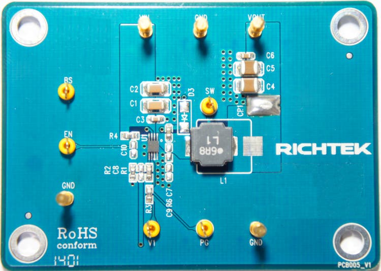
<h3>Headers Description and Placement</h3> <p class="MsoNormal"><a href="/content/dam/richtek-eds/resources/evaluation-boards/evb_rt8297bzqw/html-images/image001_en.jpg" class="fancybox"><img width="425" height="302" width="425" height="302" id="圖片 1" alt="Technical Document Image Preview" src="/content/dam/richtek-eds/resources/evaluation-boards/evb_rt8297bzqw/html-images/image001_en.jpg" /></a></p> <p class="1">Please carefully inspect the EVB IC and external components, comparing them to the following Bill of Materials, to ensure that all components are installed and undamaged. If any components are missing or damaged during transportation, please contact the distributor or send e-mail to <a href="mailto:evb_service@richtek.com" class="link">evb_service@richtek.com</a>.</p> <h3>Test Points</h3> <p class="MsoNormal">The EVB is provided with the test points and pin names listed in the table below.</p> <div> <table class="MsoNormalTable" border="1" cellspacing="0" cellpadding="0" width="680" style="width:510.2pt;border-collapse:collapse;border:none"> <tr style="height:17.0pt"> <td width="76" style="width:2.0cm;border:solid #009EB8 1.0pt;background:#009EB8; padding:0cm 5.4pt 0cm 5.4pt;height:17.0pt"> <p class="1CxSpFirst">Test point/</p> <p class="1CxSpMiddle">Pin name</p> </td> <td width="161" style="width:120.65pt;border:solid #009EB8 1.0pt;border-left: none;background:#009EB8;padding:0cm 5.4pt 0cm 5.4pt;height:17.0pt"> <p class="1CxSpMiddle">Signal</p> </td> <td width="397" style="width:297.5pt;border:solid #009EB8 1.0pt;border-left: none;background:#009EB8;padding:0cm 5.4pt 0cm 5.4pt;height:17.0pt"> <p class="1CxSpLast">Comment (expected waveforms or voltage levels on test points)</p> </td> </tr> <tr style="height:17.0pt"> <td width="76" style="width:2.0cm;border:solid #009EB8 1.0pt;border-top:none; padding:0cm 5.4pt 0cm 5.4pt;height:17.0pt"> <p class="ListParagraph1CxSpFirst">VIN</p> </td> <td width="161" style="width:120.65pt;border-top:none;border-left:none; border-bottom:solid #009EB8 1.0pt;border-right:solid #009EB8 1.0pt; padding:0cm 5.4pt 0cm 5.4pt;height:17.0pt"> <p class="ListParagraph1CxSpMiddle">Input voltage</p> </td> <td width="397" style="width:297.5pt;border-top:none;border-left:none; border-bottom:solid #009EB8 1.0pt;border-right:solid #009EB8 1.0pt; padding:0cm 5.4pt 0cm 5.4pt;height:17.0pt"> <p class="ListParagraph1CxSpLast">Input voltage range= 4V to 17V</p> </td> </tr> <tr style="height:17.0pt"> <td width="76" style="width:2.0cm;border:solid #009EB8 1.0pt;border-top:none; padding:0cm 5.4pt 0cm 5.4pt;height:17.0pt"> <p class="ListParagraph1CxSpFirst">VOUT</p> </td> <td width="161" style="width:120.65pt;border-top:none;border-left:none; border-bottom:solid #009EB8 1.0pt;border-right:solid #009EB8 1.0pt; padding:0cm 5.4pt 0cm 5.4pt;height:17.0pt"> <p class="ListParagraph1CxSpMiddle">Output voltage </p> </td> <td width="397" style="width:297.5pt;border-top:none;border-left:none; border-bottom:solid #009EB8 1.0pt;border-right:solid #009EB8 1.0pt; padding:0cm 5.4pt 0cm 5.4pt;height:17.0pt"> <p class="ListParagraph1CxSpMiddle">Default output voltage = 3.3V</p> <p class="ListParagraph1CxSpMiddle">Output voltage range= 0.8V to 12V </p> <p class="ListParagraph1CxSpLast">(see ‘’ Output Voltage Setting’’ section for changing output voltage level)</p> </td> </tr> <tr style="height:17.0pt"> <td width="76" style="width:2.0cm;border:solid #009EB8 1.0pt;border-top:none; padding:0cm 5.4pt 0cm 5.4pt;height:17.0pt"> <p class="ListParagraph1CxSpFirst">SW</p> </td> <td width="161" style="width:120.65pt;border-top:none;border-left:none; border-bottom:solid #009EB8 1.0pt;border-right:solid #009EB8 1.0pt; padding:0cm 5.4pt 0cm 5.4pt;height:17.0pt"> <p class="ListParagraph1CxSpMiddle">Switching node test point</p> </td> <td width="397" style="width:297.5pt;border-top:none;border-left:none; border-bottom:solid #009EB8 1.0pt;border-right:solid #009EB8 1.0pt; padding:0cm 5.4pt 0cm 5.4pt;height:17.0pt"> <p class="ListParagraph1CxSpLast">SW waveform</p> </td> </tr> <tr style="height:17.0pt"> <td width="76" style="width:2.0cm;border:solid #009EB8 1.0pt;border-top:none; padding:0cm 5.4pt 0cm 5.4pt;height:17.0pt"> <p class="ListParagraph1CxSpFirst">EN</p> </td> <td width="161" style="width:120.65pt;border-top:none;border-left:none; border-bottom:solid #009EB8 1.0pt;border-right:solid #009EB8 1.0pt; padding:0cm 5.4pt 0cm 5.4pt;height:17.0pt"> <p class="ListParagraph1CxSpMiddle">Enable test point</p> </td> <td width="397" style="width:297.5pt;border-top:none;border-left:none; border-bottom:solid #009EB8 1.0pt;border-right:solid #009EB8 1.0pt; padding:0cm 5.4pt 0cm 5.4pt;height:17.0pt"> <p class="ListParagraph1CxSpLast">Enable signal. EN is automatically pulled high (by R4) to enable operation. Connect EN low to disable operation.</p> </td> </tr> <tr style="height:17.0pt"> <td width="76" style="width:2.0cm;border:solid #009EB8 1.0pt;border-top:none; padding:0cm 5.4pt 0cm 5.4pt;height:17.0pt"> <p class="ListParagraph1CxSpFirst">BS</p> </td> <td width="161" style="width:120.65pt;border-top:none;border-left:none; border-bottom:solid #009EB8 1.0pt;border-right:solid #009EB8 1.0pt; padding:0cm 5.4pt 0cm 5.4pt;height:17.0pt"> <p class="ListParagraph1CxSpMiddle">Boot strap supply test point</p> </td> <td width="397" style="width:297.5pt;border-top:none;border-left:none; border-bottom:solid #009EB8 1.0pt;border-right:solid #009EB8 1.0pt; padding:0cm 5.4pt 0cm 5.4pt;height:17.0pt"> <p class="ListParagraph1CxSpLast">Floating supply voltage for the high-side N-MOSFET switch</p> </td> </tr> <tr style="height:17.0pt"> <td width="76" style="width:2.0cm;border:solid #009EB8 1.0pt;border-top:none; padding:0cm 5.4pt 0cm 5.4pt;height:17.0pt"> <p class="ListParagraph1CxSpFirst">PG</p> </td> <td width="161" style="width:120.65pt;border-top:none;border-left:none; border-bottom:solid #009EB8 1.0pt;border-right:solid #009EB8 1.0pt; padding:0cm 5.4pt 0cm 5.4pt;height:17.0pt"> <p class="ListParagraph1CxSpMiddle">Power Good test point</p> </td> <td width="397" style="width:297.5pt;border-top:none;border-left:none; border-bottom:solid #009EB8 1.0pt;border-right:solid #009EB8 1.0pt; padding:0cm 5.4pt 0cm 5.4pt;height:17.0pt"> <p class="ListParagraph1CxSpLast">Power Good Indicator</p> </td> </tr> <tr style="height:17.0pt"> <td width="76" style="width:2.0cm;border:solid #009EB8 1.0pt;border-top:none; padding:0cm 5.4pt 0cm 5.4pt;height:17.0pt"> <p class="ListParagraph1CxSpFirst">V1</p> </td> <td width="161" style="width:120.65pt;border-top:none;border-left:none; border-bottom:solid #009EB8 1.0pt;border-right:solid #009EB8 1.0pt; padding:0cm 5.4pt 0cm 5.4pt;height:17.0pt"> <p class="ListParagraph1CxSpMiddle">External Voltage for PG</p> </td> <td width="397" style="width:297.5pt;border-top:none;border-left:none; border-bottom:solid #009EB8 1.0pt;border-right:solid #009EB8 1.0pt; padding:0cm 5.4pt 0cm 5.4pt;height:17.0pt"> <p class="ListParagraph1CxSpLast">External voltage terminal for PG pull-up voltage.</p> </td> </tr> <tr style="height:17.0pt"> <td width="76" style="width:2.0cm;border:solid #009EB8 1.0pt;border-top:none; padding:0cm 5.4pt 0cm 5.4pt;height:17.0pt"> <p class="ListParagraph1CxSpFirst">GND</p> </td> <td width="161" style="width:120.65pt;border-top:none;border-left:none; border-bottom:solid #009EB8 1.0pt;border-right:solid #009EB8 1.0pt; padding:0cm 5.4pt 0cm 5.4pt;height:17.0pt"> <p class="ListParagraph1CxSpMiddle">Ground</p> </td> <td width="397" style="width:297.5pt;border-top:none;border-left:none; border-bottom:solid #009EB8 1.0pt;border-right:solid #009EB8 1.0pt; padding:0cm 5.4pt 0cm 5.4pt;height:17.0pt"> <p class="ListParagraph1CxSpLast">Ground</p> </td> </tr> </table> </div> <h3>Power-up & Measurement Procedure</h3> <p class="MsoNormal">1.Apply a 12V nominal input power supply (4V < V<sub>IN</sub> < 17V) to the VIN and GND terminals.</p> <p class="MsoNormal">2.The EN voltage is pulled to logic high by R4 (100kΩ to VIN) to enable operation. Drive EN high (>2.5V) to enable operation or low (<0.4V) to disable operation.</p> <p class="MsoNormal">3.Verify the output voltage (approximately 3.3V) between VOUT and GND.</p> <p class="MsoNormal">4.Connect an external load up to 1.5A to the VOUT and GND terminals and verify the output voltage and current. </p> <h3>Output Voltage Setting</h3> <p class="MsoNormal">Set the output voltage with the resistive divider (R1, R2) between VOUT and GND with the midpoint connected to FB. The output is set by the following formula:</p> <p class="MsoNormal"><a href="/content/dam/richtek-eds/resources/evaluation-boards/evb_rt8297bzqw/html-images/image003_en.png" class="fancybox"><img width="140" height="36" width="140" height="36" style="border-width: 0px; border-style: solid;" alt="Technical Document Image Preview" src="/content/dam/richtek-eds/resources/evaluation-boards/evb_rt8297bzqw/html-images/image003_en.png" /></a> </p> <p class="MsoNormal">The installed V<sub>OUT</sub> capacitors (C4, C5) are 22μF, 16V X5R ceramic types. Do not exceed their operating voltage range and consider their voltage coefficient (capacitance vs. bias voltage) and ensure that the capacitance is sufficient to maintain stability and provide sufficient transient response for your application. This can be verified by checking the output transient response as described in the RT8297 IC datasheet.</p>
4. Schematic, Bill of Materials and Board Layout
<h3>EVB Schematic Diagram</h3> <p class="MsoNormal"><a href="/content/dam/richtek-eds/resources/evaluation-boards/evb_rt8297bzqw/html-images/image004_en.png" class="fancybox"><img width="680" height="234" width="680" height="234" id="圖片 4" style="border-width: 0px; border-style: solid;" alt="Technical Document Image Preview" src="/content/dam/richtek-eds/resources/evaluation-boards/evb_rt8297bzqw/html-images/image004_en.png" /></a></p> <p class="MsoNormal">C1, C2: 10μF/50V/X5R, 1206, TDK C3216X5R1H106K</p> <p class="MsoNormal">C4, C5: 22μF/16V/X5R, 1210, Murata GRM32ER61C226K</p> <p class="MsoNormal">L1: 6.8μH TAIYO YUDEN NR8040T6R8N, DCR=25mΩ</p> <h3>Bill of Materials</h3> <table class="MsoNormalTable" border="1" cellspacing="0" cellpadding="0" width="680" style="border-collapse:collapse;border:none"> <tr style="height:17.0pt"> <td width="70" style="width:52.45pt;border:solid #009EB8 1.0pt;background:#009EB8; padding:0cm 1.4pt 0cm 1.4pt;height:17.0pt"> <p class="MsoNormal">Reference</p> </td> <td width="36" style="width:27.05pt;border:solid #009EB8 1.0pt;border-left: none;background:#009EB8;padding:0cm 1.4pt 0cm 1.4pt;height:17.0pt"> <p class="MsoNormal">Qty</p> </td> <td width="161" style="width:120.55pt;border:solid #009EB8 1.0pt;border-left: none;background:#009EB8;padding:0cm 1.4pt 0cm 1.4pt;height:17.0pt"> <p class="MsoNormal">Part number</p> </td> <td width="189" style="width:141.85pt;border:solid #009EB8 1.0pt;border-left: none;background:#009EB8;padding:0cm 1.4pt 0cm 1.4pt;height:17.0pt"> <p class="MsoNormal">Description</p> </td> <td width="102" style="width:76.15pt;border:solid #009EB8 1.0pt;border-left: none;background:#009EB8;padding:0cm 1.4pt 0cm 1.4pt;height:17.0pt"> <p class="MsoNormal">Package</p> </td> <td width="123" style="width:92.15pt;border:solid #009EB8 1.0pt;border-left: none;background:#009EB8;padding:0cm 1.4pt 0cm 1.4pt;height:17.0pt"> <p class="MsoNormal">Manufacture</p> </td> </tr> <tr style="height:17.0pt"> <td width="70" style="width:52.45pt;border:solid #009EB8 1.0pt;border-top:none; padding:0cm 1.4pt 0cm 1.4pt;height:17.0pt"> <p class="MsoNormal">U1</p> </td> <td width="36" style="width:27.05pt;border-top:none;border-left:none; border-bottom:solid #009EB8 1.0pt;border-right:solid #009EB8 1.0pt; padding:0cm 1.4pt 0cm 1.4pt;height:17.0pt"> <p class="MsoNormal">1</p> </td> <td width="161" style="width:120.55pt;border-top:none;border-left:none; border-bottom:solid #009EB8 1.0pt;border-right:solid #009EB8 1.0pt; padding:0cm 1.4pt 0cm 1.4pt;height:17.0pt"> <p class="MsoNormal">RT8297BZQW</p> </td> <td width="189" style="width:141.85pt;border-top:none;border-left:none; border-bottom:solid #009EB8 1.0pt;border-right:solid #009EB8 1.0pt; padding:0cm 1.4pt 0cm 1.4pt;height:17.0pt"> <p class="MsoNormal">DC-DC Converter</p> </td> <td width="102" style="width:76.15pt;border-top:none;border-left:none; border-bottom:solid #009EB8 1.0pt;border-right:solid #009EB8 1.0pt; padding:0cm 1.4pt 0cm 1.4pt;height:17.0pt"> <p class="MsoNormal">WDFN-8L 2x2</p> </td> <td width="123" style="width:92.15pt;border-top:none;border-left:none; border-bottom:solid #009EB8 1.0pt;border-right:solid #009EB8 1.0pt; padding:0cm 1.4pt 0cm 1.4pt;height:17.0pt"> <p class="MsoNormal">Richtek</p> </td> </tr> <tr style="height:34.5pt"> <td width="70" style="width:52.45pt;border:solid #009EB8 1.0pt;border-top:none; padding:0cm 1.4pt 0cm 1.4pt;height:34.5pt"> <p class="MsoNormal">C1, C2</p> </td> <td width="36" style="width:27.05pt;border-top:none;border-left:none; border-bottom:solid #009EB8 1.0pt;border-right:solid #009EB8 1.0pt; padding:0cm 1.4pt 0cm 1.4pt;height:34.5pt"> <p class="MsoNormal">2</p> </td> <td width="161" style="width:120.55pt;border-top:none;border-left:none; border-bottom:solid #009EB8 1.0pt;border-right:solid #009EB8 1.0pt; padding:0cm 1.4pt 0cm 1.4pt;height:34.5pt"> <p class="MsoNormal">C3216X5R1H106K160AB</p> </td> <td width="189" style="width:141.85pt;border-top:none;border-left:none; border-bottom:solid #009EB8 1.0pt;border-right:solid #009EB8 1.0pt; padding:0cm 1.4pt 0cm 1.4pt;height:34.5pt"> <p class="MsoNormal">10μF/±10%/50V/X5R</p> <p class="MsoNormal">Ceramic Capacitor</p> </td> <td width="102" style="width:76.15pt;border-top:none;border-left:none; border-bottom:solid #009EB8 1.0pt;border-right:solid #009EB8 1.0pt; padding:0cm 1.4pt 0cm 1.4pt;height:34.5pt"> <p class="MsoNormal">1206</p> </td> <td width="123" style="width:92.15pt;border-top:none;border-left:none; border-bottom:solid #009EB8 1.0pt;border-right:solid #009EB8 1.0pt; padding:0cm 1.4pt 0cm 1.4pt;height:34.5pt"> <p class="MsoNormal">TDK</p> </td> </tr> <tr style="height:34.5pt"> <td width="70" style="width:52.45pt;border:solid #009EB8 1.0pt;border-top:none; padding:0cm 1.4pt 0cm 1.4pt;height:34.5pt"> <p class="MsoNormal">C4, C5</p> </td> <td width="36" style="width:27.05pt;border-top:none;border-left:none; border-bottom:solid #009EB8 1.0pt;border-right:solid #009EB8 1.0pt; padding:0cm 1.4pt 0cm 1.4pt;height:34.5pt"> <p class="MsoNormal">2</p> </td> <td width="161" style="width:120.55pt;border-top:none;border-left:none; border-bottom:solid #009EB8 1.0pt;border-right:solid #009EB8 1.0pt; padding:0cm 1.4pt 0cm 1.4pt;height:34.5pt"> <p class="MsoNormal">GRM32ER61C226KE20#</p> </td> <td width="189" style="width:141.85pt;border-top:none;border-left:none; border-bottom:solid #009EB8 1.0pt;border-right:solid #009EB8 1.0pt; padding:0cm 1.4pt 0cm 1.4pt;height:34.5pt"> <p class="MsoNormal">22μF/±10%/16V/X5R</p> <p class="MsoNormal">Ceramic Capacitor</p> </td> <td width="102" style="width:76.15pt;border-top:none;border-left:none; border-bottom:solid #009EB8 1.0pt;border-right:solid #009EB8 1.0pt; padding:0cm 1.4pt 0cm 1.4pt;height:34.5pt"> <p class="MsoNormal">1210</p> </td> <td width="123" style="width:92.15pt;border-top:none;border-left:none; border-bottom:solid #009EB8 1.0pt;border-right:solid #009EB8 1.0pt; padding:0cm 1.4pt 0cm 1.4pt;height:34.5pt"> <p class="MsoNormal">Murata</p> </td> </tr> <tr style="height:34.5pt"> <td width="70" style="width:52.45pt;border:solid #009EB8 1.0pt;border-top:none; padding:0cm 1.4pt 0cm 1.4pt;height:34.5pt"> <p class="MsoNormal">C7</p> </td> <td width="36" style="width:27.05pt;border-top:none;border-left:none; border-bottom:solid #009EB8 1.0pt;border-right:solid #009EB8 1.0pt; padding:0cm 1.4pt 0cm 1.4pt;height:34.5pt"> <p class="MsoNormal">1</p> </td> <td width="161" style="width:120.55pt;border-top:none;border-left:none; border-bottom:solid #009EB8 1.0pt;border-right:solid #009EB8 1.0pt; padding:0cm 1.4pt 0cm 1.4pt;height:34.5pt"> <p class="MsoNormal">GRM32MR71H103KA01#</p> </td> <td width="189" style="width:141.85pt;border-top:none;border-left:none; border-bottom:solid #009EB8 1.0pt;border-right:solid #009EB8 1.0pt; padding:0cm 1.4pt 0cm 1.4pt;height:34.5pt"> <p class="MsoNormal">10nF/±10%/50V/X7R</p> <p class="MsoNormal">Ceramic Capacitor</p> </td> <td width="102" style="width:76.15pt;border-top:none;border-left:none; border-bottom:solid #009EB8 1.0pt;border-right:solid #009EB8 1.0pt; padding:0cm 1.4pt 0cm 1.4pt;height:34.5pt"> <p class="MsoNormal">0603</p> </td> <td width="123" style="width:92.15pt;border-top:none;border-left:none; border-bottom:solid #009EB8 1.0pt;border-right:solid #009EB8 1.0pt; padding:0cm 1.4pt 0cm 1.4pt;height:34.5pt"> <p class="MsoNormal">Murata</p> </td> </tr> <tr style="height:34.5pt"> <td width="70" style="width:52.45pt;border:solid #009EB8 1.0pt;border-top:none; padding:0cm 1.4pt 0cm 1.4pt;height:34.5pt"> <p class="MsoNormal">C3, C6</p> </td> <td width="36" style="width:27.05pt;border-top:none;border-left:none; border-bottom:solid #009EB8 1.0pt;border-right:solid #009EB8 1.0pt; padding:0cm 1.4pt 0cm 1.4pt;height:34.5pt"> <p class="MsoNormal">2</p> </td> <td width="161" style="width:120.55pt;border-top:none;border-left:none; border-bottom:solid #009EB8 1.0pt;border-right:solid #009EB8 1.0pt; padding:0cm 1.4pt 0cm 1.4pt;height:34.5pt"> <p class="MsoNormal">C1608X7R1H104K080AA</p> </td> <td width="189" style="width:141.85pt;border-top:none;border-left:none; border-bottom:solid #009EB8 1.0pt;border-right:solid #009EB8 1.0pt; padding:0cm 1.4pt 0cm 1.4pt;height:34.5pt"> <p class="MsoNormal">0.1μF/±10%/50V/X7R</p> <p class="MsoNormal">Ceramic Capacitor</p> </td> <td width="102" style="width:76.15pt;border-top:none;border-left:none; border-bottom:solid #009EB8 1.0pt;border-right:solid #009EB8 1.0pt; padding:0cm 1.4pt 0cm 1.4pt;height:34.5pt"> <p class="MsoNormal">0603</p> </td> <td width="123" style="width:92.15pt;border-top:none;border-left:none; border-bottom:solid #009EB8 1.0pt;border-right:solid #009EB8 1.0pt; padding:0cm 1.4pt 0cm 1.4pt;height:34.5pt"> <p class="MsoNormal">TDK</p> </td> </tr> <tr style="height:17.0pt"> <td width="70" style="width:52.45pt;border:solid #009EB8 1.0pt;border-top:none; padding:0cm 1.4pt 0cm 1.4pt;height:17.0pt"> <p class="MsoNormal">C8, C9, C10</p> </td> <td width="36" style="width:27.05pt;border-top:none;border-left:none; border-bottom:solid #009EB8 1.0pt;border-right:solid #009EB8 1.0pt; padding:0cm 1.4pt 0cm 1.4pt;height:17.0pt"> <p class="MsoNormal">0</p> </td> <td width="161" style="width:120.55pt;border-top:none;border-left:none; border-bottom:solid #009EB8 1.0pt;border-right:solid #009EB8 1.0pt; padding:0cm 1.4pt 0cm 1.4pt;height:17.0pt"></td> <td width="189" style="width:141.85pt;border-top:none;border-left:none; border-bottom:solid #009EB8 1.0pt;border-right:solid #009EB8 1.0pt; padding:0cm 1.4pt 0cm 1.4pt;height:17.0pt"> <p class="MsoNormal">Not Installed</p> </td> <td width="102" style="width:76.15pt;border-top:none;border-left:none; border-bottom:solid #009EB8 1.0pt;border-right:solid #009EB8 1.0pt; padding:0cm 1.4pt 0cm 1.4pt;height:17.0pt"> <p class="MsoNormal">0603</p> </td> <td width="123" style="width:92.15pt;border-top:none;border-left:none; border-bottom:solid #009EB8 1.0pt;border-right:solid #009EB8 1.0pt; padding:0cm 1.4pt 0cm 1.4pt;height:17.0pt"></td> </tr> <tr style="height:17.0pt"> <td width="70" style="width:52.45pt;border:solid #009EB8 1.0pt;border-top:none; padding:0cm 1.4pt 0cm 1.4pt;height:17.0pt"> <p class="MsoNormal">L1</p> </td> <td width="36" style="width:27.05pt;border-top:none;border-left:none; border-bottom:solid #009EB8 1.0pt;border-right:solid #009EB8 1.0pt; padding:0cm 1.4pt 0cm 1.4pt;height:17.0pt"> <p class="MsoNormal">1</p> </td> <td width="161" style="width:120.55pt;border-top:none;border-left:none; border-bottom:solid #009EB8 1.0pt;border-right:solid #009EB8 1.0pt; padding:0cm 1.4pt 0cm 1.4pt;height:17.0pt"> <p class="MsoNormal">NR8040T6R8N</p> </td> <td width="189" style="width:141.85pt;border-top:none;border-left:none; border-bottom:solid #009EB8 1.0pt;border-right:solid #009EB8 1.0pt; padding:0cm 1.4pt 0cm 1.4pt;height:17.0pt"> <p class="MsoNormal">6.8uH/3.7A/±30%, </p> <p class="MsoNormal">DCR=25mΩ, Inductor</p> </td> <td width="102" style="width:76.15pt;border-top:none;border-left:none; border-bottom:solid #009EB8 1.0pt;border-right:solid #009EB8 1.0pt; padding:0cm 1.4pt 0cm 1.4pt;height:17.0pt"> <p class="MsoNormal">8mmx8mmx4mm</p> </td> <td width="123" style="width:92.15pt;border-top:none;border-left:none; border-bottom:solid #009EB8 1.0pt;border-right:solid #009EB8 1.0pt; padding:0cm 1.4pt 0cm 1.4pt;height:17.0pt"> <p class="MsoNormal">TAIYO YUDEN</p> </td> </tr> <tr style="height:17.0pt"> <td width="70" style="width:52.45pt;border:solid #009EB8 1.0pt;border-top:none; padding:0cm 1.4pt 0cm 1.4pt;height:17.0pt"> <p class="MsoNormal">R1</p> </td> <td width="36" style="width:27.05pt;border-top:none;border-left:none; border-bottom:solid #009EB8 1.0pt;border-right:solid #009EB8 1.0pt; padding:0cm 1.4pt 0cm 1.4pt;height:17.0pt"> <p class="MsoNormal">1</p> </td> <td width="161" style="width:120.55pt;border-top:none;border-left:none; border-bottom:solid #009EB8 1.0pt;border-right:solid #009EB8 1.0pt; padding:0cm 1.4pt 0cm 1.4pt;height:17.0pt"> </td> <td width="189" nowrap style="width:141.85pt;border-top:none;border-left:none; border-bottom:solid #009EB8 1.0pt;border-right:solid #009EB8 1.0pt; padding:0cm 1.4pt 0cm 1.4pt;height:17.0pt"> <p class="MsoNormal">47kΩ/±1%, Resistor</p> </td> <td width="102" style="width:76.15pt;border-top:none;border-left:none; border-bottom:solid #009EB8 1.0pt;border-right:solid #009EB8 1.0pt; padding:0cm 1.4pt 0cm 1.4pt;height:17.0pt"> <p class="MsoNormal">0603</p> </td> <td width="123" style="width:92.15pt;border-top:none;border-left:none; border-bottom:solid #009EB8 1.0pt;border-right:solid #009EB8 1.0pt; padding:0cm 1.4pt 0cm 1.4pt;height:17.0pt"> </td> </tr> <tr style="height:17.0pt"> <td width="70" style="width:52.45pt;border:solid #009EB8 1.0pt;border-top:none; padding:0cm 1.4pt 0cm 1.4pt;height:17.0pt"> <p class="MsoNormal">R2</p> </td> <td width="36" style="width:27.05pt;border-top:none;border-left:none; border-bottom:solid #009EB8 1.0pt;border-right:solid #009EB8 1.0pt; padding:0cm 1.4pt 0cm 1.4pt;height:17.0pt"> <p class="MsoNormal">1</p> </td> <td width="161" style="width:120.55pt;border-top:none;border-left:none; border-bottom:solid #009EB8 1.0pt;border-right:solid #009EB8 1.0pt; padding:0cm 1.4pt 0cm 1.4pt;height:17.0pt"> </td> <td width="189" nowrap style="width:141.85pt;border-top:none;border-left:none; border-bottom:solid #009EB8 1.0pt;border-right:solid #009EB8 1.0pt; padding:0cm 1.4pt 0cm 1.4pt;height:17.0pt"> <p class="MsoNormal">15kΩ/±1%, Resistor</p> </td> <td width="102" style="width:76.15pt;border-top:none;border-left:none; border-bottom:solid #009EB8 1.0pt;border-right:solid #009EB8 1.0pt; padding:0cm 1.4pt 0cm 1.4pt;height:17.0pt"> <p class="MsoNormal">0603</p> </td> <td width="123" style="width:92.15pt;border-top:none;border-left:none; border-bottom:solid #009EB8 1.0pt;border-right:solid #009EB8 1.0pt; padding:0cm 1.4pt 0cm 1.4pt;height:17.0pt"> </td> </tr> <tr style="height:17.0pt"> <td width="70" style="width:52.45pt;border:solid #009EB8 1.0pt;border-top:none; padding:0cm 1.4pt 0cm 1.4pt;height:17.0pt"> <p class="MsoNormal">R3, R4</p> </td> <td width="36" style="width:27.05pt;border-top:none;border-left:none; border-bottom:solid #009EB8 1.0pt;border-right:solid #009EB8 1.0pt; padding:0cm 1.4pt 0cm 1.4pt;height:17.0pt"> <p class="MsoNormal">1</p> </td> <td width="161" style="width:120.55pt;border-top:none;border-left:none; border-bottom:solid #009EB8 1.0pt;border-right:solid #009EB8 1.0pt; padding:0cm 1.4pt 0cm 1.4pt;height:17.0pt"> </td> <td width="189" nowrap style="width:141.85pt;border-top:none;border-left:none; border-bottom:solid #009EB8 1.0pt;border-right:solid #009EB8 1.0pt; padding:0cm 1.4pt 0cm 1.4pt;height:17.0pt"> <p class="MsoNormal">100kΩ/±1%, Resistor</p> </td> <td width="102" style="width:76.15pt;border-top:none;border-left:none; border-bottom:solid #009EB8 1.0pt;border-right:solid #009EB8 1.0pt; padding:0cm 1.4pt 0cm 1.4pt;height:17.0pt"> <p class="MsoNormal">0603</p> </td> <td width="123" style="width:92.15pt;border-top:none;border-left:none; border-bottom:solid #009EB8 1.0pt;border-right:solid #009EB8 1.0pt; padding:0cm 1.4pt 0cm 1.4pt;height:17.0pt"> </td> </tr> <tr style="height:17.0pt"> <td width="70" style="width:52.45pt;border:solid #009EB8 1.0pt;border-top:none; padding:0cm 1.4pt 0cm 1.4pt;height:17.0pt"> <p class="MsoNormal">CP1</p> </td> <td width="36" style="width:27.05pt;border-top:none;border-left:none; border-bottom:solid #009EB8 1.0pt;border-right:solid #009EB8 1.0pt; padding:0cm 1.4pt 0cm 1.4pt;height:17.0pt"> <p class="MsoNormal">1</p> </td> <td width="161" style="width:120.55pt;border-top:none;border-left:none; border-bottom:solid #009EB8 1.0pt;border-right:solid #009EB8 1.0pt; padding:0cm 1.4pt 0cm 1.4pt;height:17.0pt"></td> <td width="189" nowrap style="width:141.85pt;border-top:none;border-left:none; border-bottom:solid #009EB8 1.0pt;border-right:solid #009EB8 1.0pt; padding:0cm 1.4pt 0cm 1.4pt;height:17.0pt"> <p class="MsoNormal">Short</p> </td> <td width="102" style="width:76.15pt;border-top:none;border-left:none; border-bottom:solid #009EB8 1.0pt;border-right:solid #009EB8 1.0pt; padding:0cm 1.4pt 0cm 1.4pt;height:17.0pt"></td> <td width="123" style="width:92.15pt;border-top:none;border-left:none; border-bottom:solid #009EB8 1.0pt;border-right:solid #009EB8 1.0pt; padding:0cm 1.4pt 0cm 1.4pt;height:17.0pt"></td> </tr> <tr style="height:17.0pt"> <td width="70" style="width:52.45pt;border:solid #009EB8 1.0pt;border-top:none; padding:0cm 1.4pt 0cm 1.4pt;height:17.0pt"> <p class="MsoNormal">D3, R6</p> </td> <td width="36" style="width:27.05pt;border-top:none;border-left:none; border-bottom:solid #009EB8 1.0pt;border-right:solid #009EB8 1.0pt; padding:0cm 1.4pt 0cm 1.4pt;height:17.0pt"> <p class="MsoNormal">0</p> </td> <td width="161" style="width:120.55pt;border-top:none;border-left:none; border-bottom:solid #009EB8 1.0pt;border-right:solid #009EB8 1.0pt; padding:0cm 1.4pt 0cm 1.4pt;height:17.0pt"></td> <td width="189" style="width:141.85pt;border-top:none;border-left:none; border-bottom:solid #009EB8 1.0pt;border-right:solid #009EB8 1.0pt; padding:0cm 1.4pt 0cm 1.4pt;height:17.0pt"> <p class="MsoNormal">Not Installed</p> </td> <td width="102" style="width:76.15pt;border-top:none;border-left:none; border-bottom:solid #009EB8 1.0pt;border-right:solid #009EB8 1.0pt; padding:0cm 1.4pt 0cm 1.4pt;height:17.0pt"></td> <td width="123" style="width:92.15pt;border-top:none;border-left:none; border-bottom:solid #009EB8 1.0pt;border-right:solid #009EB8 1.0pt; padding:0cm 1.4pt 0cm 1.4pt;height:17.0pt"></td> </tr> <tr style="height:17.0pt"> <td width="70" style="width:52.45pt;border:solid #009EB8 1.0pt;border-top:none; padding:0cm 1.4pt 0cm 1.4pt;height:17.0pt"> <p class="MsoNormal">TP</p> </td> <td width="36" style="width:27.05pt;border-top:none;border-left:none; border-bottom:solid #009EB8 1.0pt;border-right:solid #009EB8 1.0pt; padding:0cm 1.4pt 0cm 1.4pt;height:17.0pt"> <p class="MsoNormal">6</p> </td> <td width="161" style="width:120.55pt;border-top:none;border-left:none; border-bottom:solid #009EB8 1.0pt;border-right:solid #009EB8 1.0pt; padding:0cm 1.4pt 0cm 1.4pt;height:17.0pt"></td> <td width="189" style="width:141.85pt;border-top:none;border-left:none; border-bottom:solid #009EB8 1.0pt;border-right:solid #009EB8 1.0pt; padding:0cm 1.4pt 0cm 1.4pt;height:17.0pt"> <p class="MsoNormal">Test Pin</p> </td> <td width="102" style="width:76.15pt;border-top:none;border-left:none; border-bottom:solid #009EB8 1.0pt;border-right:solid #009EB8 1.0pt; padding:0cm 1.4pt 0cm 1.4pt;height:17.0pt"></td> <td width="123" style="width:92.15pt;border-top:none;border-left:none; border-bottom:solid #009EB8 1.0pt;border-right:solid #009EB8 1.0pt; padding:0cm 1.4pt 0cm 1.4pt;height:17.0pt"></td> </tr> <tr style="height:17.0pt"> <td width="70" style="width:52.45pt;border:solid #009EB8 1.0pt;border-top:none; padding:0cm 1.4pt 0cm 1.4pt;height:17.0pt"> <p class="MsoNormal">GP</p> </td> <td width="36" style="width:27.05pt;border-top:none;border-left:none; border-bottom:solid #009EB8 1.0pt;border-right:solid #009EB8 1.0pt; padding:0cm 1.4pt 0cm 1.4pt;height:17.0pt"> <p class="MsoNormal">4</p> </td> <td width="161" style="width:120.55pt;border-top:none;border-left:none; border-bottom:solid #009EB8 1.0pt;border-right:solid #009EB8 1.0pt; padding:0cm 1.4pt 0cm 1.4pt;height:17.0pt"></td> <td width="189" style="width:141.85pt;border-top:none;border-left:none; border-bottom:solid #009EB8 1.0pt;border-right:solid #009EB8 1.0pt; padding:0cm 1.4pt 0cm 1.4pt;height:17.0pt"> <p class="MsoNormal">Golden Pin</p> </td> <td width="102" style="width:76.15pt;border-top:none;border-left:none; border-bottom:solid #009EB8 1.0pt;border-right:solid #009EB8 1.0pt; padding:0cm 1.4pt 0cm 1.4pt;height:17.0pt"></td> <td width="123" style="width:92.15pt;border-top:none;border-left:none; border-bottom:solid #009EB8 1.0pt;border-right:solid #009EB8 1.0pt; padding:0cm 1.4pt 0cm 1.4pt;height:17.0pt"></td> </tr> </table> <h3>EVB Layout</h3> <p class="1CxSpFirst"><a href="/content/dam/richtek-eds/resources/evaluation-boards/evb_rt8297bzqw/html-images/image005_en.png" class="fancybox"><img width="495" height="354" width="495" height="354" id="圖片 5" style="border-width: 0px; border-style: solid;" alt="Technical Document Image Preview" src="/content/dam/richtek-eds/resources/evaluation-boards/evb_rt8297bzqw/html-images/image005_en.png" /></a></p> <p class="1CxSpMiddle">Top View (1<sup>st</sup>layer)</p> <p class="1CxSpMiddle"><a href="/content/dam/richtek-eds/resources/evaluation-boards/evb_rt8297bzqw/html-images/image006_en.png" class="fancybox"><img width="495" height="354" width="495" height="354" id="圖片 6" style="border-width: 0px; border-style: solid;" alt="Technical Document Image Preview" src="/content/dam/richtek-eds/resources/evaluation-boards/evb_rt8297bzqw/html-images/image006_en.png" /></a></p> <p class="1CxSpLast">Bottom View (4<sup>th</sup> Layer)</p> <p class="1CxSpFirst"><a href="/content/dam/richtek-eds/resources/evaluation-boards/evb_rt8297bzqw/html-images/image007_en.png" class="fancybox"><img width="430" height="306" width="430" height="306" id="圖片 7" style="border-width: 0px; border-style: solid;" alt="Technical Document Image Preview" src="/content/dam/richtek-eds/resources/evaluation-boards/evb_rt8297bzqw/html-images/image007_en.png" /></a></p> <p class="1CxSpMiddle">Component Placement Guide—Component Side (1<sup>st</sup>layer)</p> <p class="1CxSpMiddle"><a href="/content/dam/richtek-eds/resources/evaluation-boards/evb_rt8297bzqw/html-images/image008_en.png" class="fancybox"><img width="432" height="308" width="432" height="308" id="圖片 8" style="border-width: 0px; border-style: solid;" alt="Technical Document Image Preview" src="/content/dam/richtek-eds/resources/evaluation-boards/evb_rt8297bzqw/html-images/image008_en.png" /></a></p> <p class="1CxSpMiddle">PCB Layout—Component Side (1<sup>st</sup>Layer)</p> <p class="1CxSpMiddle"><a href="/content/dam/richtek-eds/resources/evaluation-boards/evb_rt8297bzqw/html-images/image009_en.png" class="fancybox"><img width="430" height="309" width="430" height="309" id="圖片 9" style="border-width: 0px; border-style: solid;" alt="Technical Document Image Preview" src="/content/dam/richtek-eds/resources/evaluation-boards/evb_rt8297bzqw/html-images/image009_en.png" /></a></p> <p class="1CxSpMiddle">PCB Layout—Inner Side (2<sup>nd</sup>layer)</p> <p class="1CxSpMiddle"><a href="/content/dam/richtek-eds/resources/evaluation-boards/evb_rt8297bzqw/html-images/image010_en.png" class="fancybox"><img width="431" height="308" width="431" height="308" id="圖片 10" style="border-width: 0px; border-style: solid;" alt="Technical Document Image Preview" src="/content/dam/richtek-eds/resources/evaluation-boards/evb_rt8297bzqw/html-images/image010_en.png" /></a></p> <p class="1CxSpMiddle">PCB Layout—Inner Side (3<sup>rd</sup> layer)</p> <p class="1CxSpMiddle"><a href="/content/dam/richtek-eds/resources/evaluation-boards/evb_rt8297bzqw/html-images/image011_en.png" class="fancybox"><img width="441" height="314" width="441" height="314" id="圖片 11" style="border-width: 0px; border-style: solid;" alt="Technical Document Image Preview" src="/content/dam/richtek-eds/resources/evaluation-boards/evb_rt8297bzqw/html-images/image011_en.png" /></a></p> <p class="1CxSpMiddle">Component Placement Guide—Bottom Side (4<sup>th</sup> Layer)</p> <p class="1CxSpMiddle"><a href="/content/dam/richtek-eds/resources/evaluation-boards/evb_rt8297bzqw/html-images/image012_en.png" class="fancybox"><img width="430" height="311" width="430" height="311" id="圖片 12" style="border-width: 0px; border-style: solid;" alt="Technical Document Image Preview" src="/content/dam/richtek-eds/resources/evaluation-boards/evb_rt8297bzqw/html-images/image012_en.png" /></a></p> <p class="1CxSpLast">PCB Layout—Bottom Side (4<sup>th</sup> Layer)</p>
32
32
32
0
design-resources
designResourceMultipleTable
56
32
32
32
24
24
24
24
i18n(tabs.related-product.title)
relatedProductTabs
i18n(tab-item.parameter-section.title)
parameterSection
parameterSectionTab
i18n(tab-item.package-size-pin-size-section.title)
packageSizePinsSizeSection
packageSizePinsSizeSectionTab
i18n(tab-item.product-feature-section.title)
productFeatureSection
productFeatureSectionTab
24
24
24
24
buttonSeeProductDifferences
text-with-icon
right
secondary-m
tertiary
i18n(button-item.see-product-differences.button-label)
i18n(button-item.see-product-differences.button-link)
_self


false
buttonFindOtherCategory
dropdown
i18n(button-item.find-other-category.button-label)
i18n(button-item.find-other-category.button-link)
_self
category-list
32
32
32
32
scrollable-table
parameterTable
normal-table
table-group
package-size-pins-size
packageSizePinsSizeTable
productFeature
24
24
24
24
i18n(tabs.ordering-information.title)
orderingInformationTabs
i18n(tab-item.evb-section.title)
evbSection
evbSectionTab
i18n(tab-item.product-section.title)
productSection
productSectionTab
24
24
24
24
evbImageSwitcher

normal-table
card-list
evb
evbTable
productImageSwitcher
normal-table
card-list
products
productTable