Powering Microcontrollers from Industrial Supply Rails
Abstract
The use of small microcontrollers like 8051, Cortex M0 or PIC16 is widespread
in many electronic devices. Powering these devices is relatively straightforward,
but in industrial environments or other applications using higher input supply
voltages, there are different methods for stepping down the input supply to
the 3.3V low current supply. Efficiency, output ripple, footprint and cost can
be important decision factors for choosing a suitable power supply solution.
This application note provides some solutions using Richtek ICs for powering
these devices from (industrial) 24V supply rails.
1. Introduction
Many applications use small microcontrollers for I/O control or communication.
The supply requirements for these microcontrollers are normally around 3.3V
with current ranging from 5 ~ 50mA, depending on peripheral I/O blocks. For
selecting the right power management topology, the designer has to consider
efficiency, output ripple, footprint and cost.
2. Voltage Step-Down Using RT9058/RT9069/RT9068 Linear Regulator
The simplest way to step down voltage is using a linear voltage regulator.
In many cases this is a good solution if load current is low and efficiency
is not important. But when the difference between Input and output voltage becomes
higher, the regulator dissipation can still become a critical factor at slightly
higher load currents. In industrial environments, input voltage fluctuations
may occur, so the regulator input range must be sufficient to handle these fluctuations.
Below table shows various Richtek linear regulators that can be used for
powering MCUs from 24V rails. The amount of load current that can be supplied
mainly depends on the thermal limitation of the package. The power dissipation
figures below are practical values that are valid in normal PCB layout with
some extra copper to the ground pins of device. 3.3V is a common output voltage,
but different voltages are available.
|
Richtek part
number
|
Description
|
Vin range
|
Package
|
Max dissipation
(TA = 60°C)
|
Max average load at 24V input
|
|
RT9058-33GV
|
2μA IQ, fixed output, without
enable
|
3.5 to 36V
|
SOT23-3
|
~ 0.25W
|
12mA
|
|
RT9058-33GX
|
2μA IQ, fixed output, without
enable
|
3.5 to 36V
|
SOT89
|
~ 0.5W
|
24mA
|
|
RT9069-33GB
|
2μA IQ, fixed output, with enable
|
3.5 to 36V
|
SOT23-5
|
~ 0.3W
|
14mA
|
|
RT9069-33GX5
|
2μA IQ, fixed output, with enable
|
3.5 to 36V
|
SOT89-5
|
~ 0.55W
|
26mA
|
|
RT9069-33GSP
|
2μA IQ, fixed output, with enable
|
3.5 to 36V
|
PSOP-8
|
~ 0.8W
|
38mA
|
|
RT9068-33GGRT9074-33GG
|
30μA IQ, fixed output, without
enable
|
4.5 to 60V
|
SOT223
|
~ 0.7W
|
33mA
|
|
RT9068GFP
RT9074GFP
RT9068-33GFP
RT9074-33GFP
|
30μA IQ, adj/fixed o/p, with
enable
|
4.5 to 60V
|
MSOP-8
|
~ 0.75W
|
33mA
|
|
RT9068GSP
RT9074GSP
RT9068-33GSP
RT9074-33GFP
|
30μA IQ, adj/fixed o/p, with
enable
|
4.5 to 60V
|
PSOP-8
|
~ 0.8W
|
38mA
|
The circuits for these linear regulators are extremely simple and ceramic
capacitors as small as 1μF can be used. Figure 1 shows some application examples.
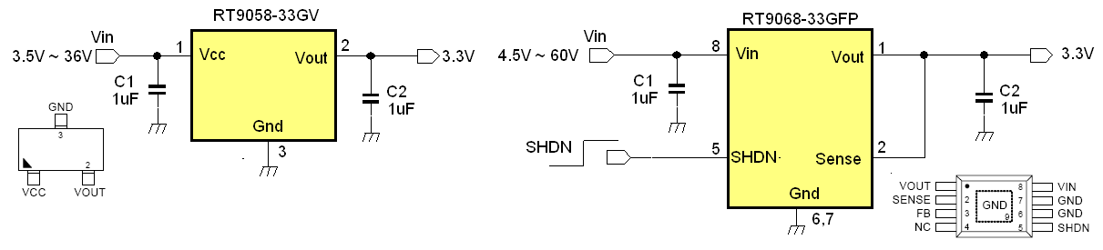
Figure 1.
The RT9058 and RT9069 have the advantage that at zero load, the regulator
consumes almost zero power due to their very low quiescent current of only 2μA.
This makes them suitable to be used with battery inputs as well.
3. Voltage Step-Down Using RT6200 Buck Converter
To achieve higher efficiency, a switching step-down regulator must be used.
Because of the low load currents in microprocessor supplies, the switching losses
of the converter play a larger role in the total efficiency than the MOSFET
conduction losses. Reducing frequency will reduce switching losses, but pulse
skipping modes sometimes have higher output voltage ripple due to the discontinuous
conduction with fixed peak current operation in this mode.
The RT6200GE is a low current asynchronous buck converter with 36V input
rating and 1.2MHz switching frequency. The SOT23-6 package achieves small application
footprint, while the high switching frequency allows the use of relatively small
inductors and output capacitors, and reduces output ripple. Block diagram and
basic schematic are shown in figure 2.
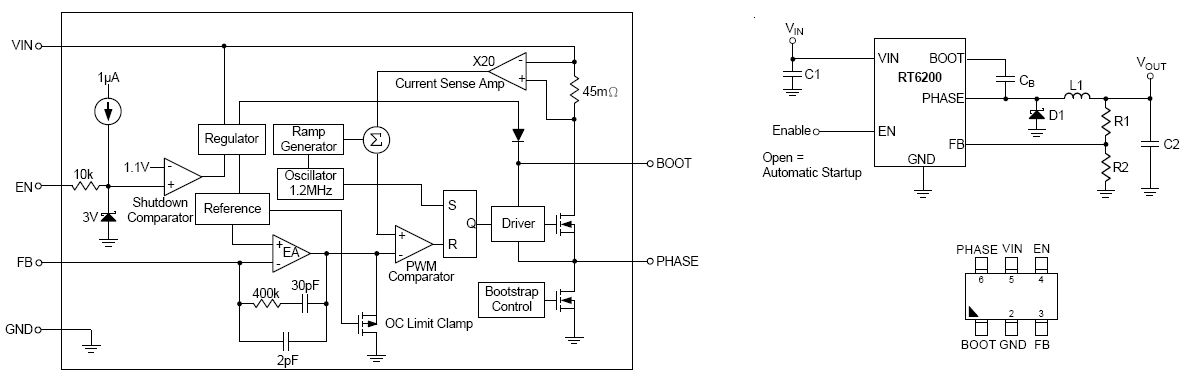
Figure 2.
In light load operation, this converter works in discontinuous mode, and
the high-side MOSFET will occasionally skip pulses, to keep output regulated.
An internal low-side MOSFET recharges the bootstrap capacitor. Small external
Schottky diodes can be used and these devices switch fast and have low voltage
drop at low current levels. This operation achieves good efficiency over wide
input and output voltage ranges.
Figure 3 below shows the complete application circuit for providing a stable
3.3V from higher input voltages.
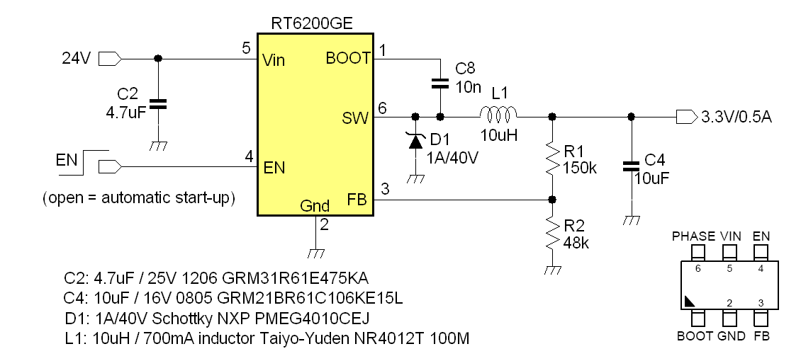
Figure 3.
The circuit is designed for load currents up to 0.5A, and uses only a few
external components. At 0.5A loads, the converter works at 1.2MHz continuous
conduction mode.
Inductor Current ripple is calculated by :
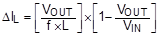 Ripple is normally set at 0.4*I-max.
Also for low current designs, it is recommended to keep the current ripple
around 0.4*device max rated current. A 10μH inductor will give 238mApp current
ripple. This means that the converter will enter discontinuous mode at load
currents lower than 119mA. At light loads, below 75mA, the converter starts
to work in pulse skip mode with fixed peak current of around 200mA.
In this design, the inductor is a small 4x4x1.2mm type, with saturation current
of 700mA. For load currents below 100mA, a smaller type with ~350mA saturation
current could be used.
The output capacitor determines the output ripple. The 10μF/16V 0805 size
MLCC has around 7.7μF capacitance at 3.3V due to DC bias effect. In pulse
skip mode, the output voltage ripple will increase to around 22mVpp.
The RT6200 has internal compensation, but since the error amplifier is a
normal OPAMP type, the bandwidth of the converter can be modified by changing
value of the upper feedback resistor R1. The compensator gain (400kΩ/R1)
is normally set at 12dB for typical applications that use 10μF output capacitance,
resulting in a bandwidth of around 70kHz. When using lower value output capacitance,
the converter bandwidth will increase. In order to keep sufficient phase margin,
the value of R1 needs to be increased. To make this design less sensitive to
noise, the bandwidth has been set slightly lower to 55kHz and phase margin is
58 degrees.
For automatic start-up, the EN pin can be left floating..
Figure 4 below shows the output voltage, switching waveform and inductor
current at 10mA and 20mA load condition. In both cases, the converter works
in pulse skip mode. The small internal low-side MOSFET will activate during
every clock cycle to re-charge the bootstrap capacitor, and this results in
some extra ring pulses between the high-side MOSFET switch cycles.
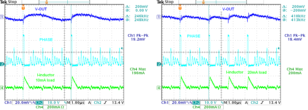
Figure 4.
The efficiency of this application is shown in figure 5. In the 50mA range,
the efficiency is around 60%.
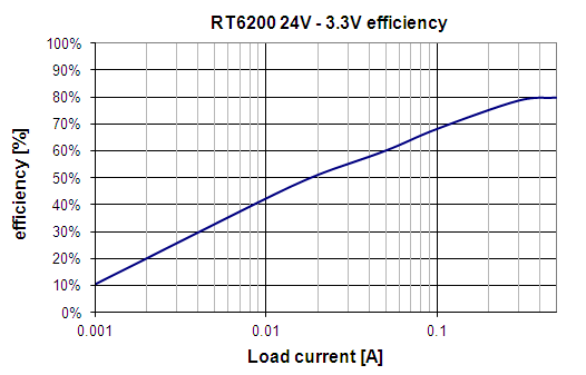
Figure 5.
An example layout is shown in figure 6. The power section is placed at the
left top corner, and several vias connect power ground to IC ground (underneath
the IC) via the inner ground layer. The feedback pin is sensitive to noise pick-up,
and the R1/R2 network should be placed close to this pin, away from noisy signals.
Total footprint of this layout is 9 x 9mm
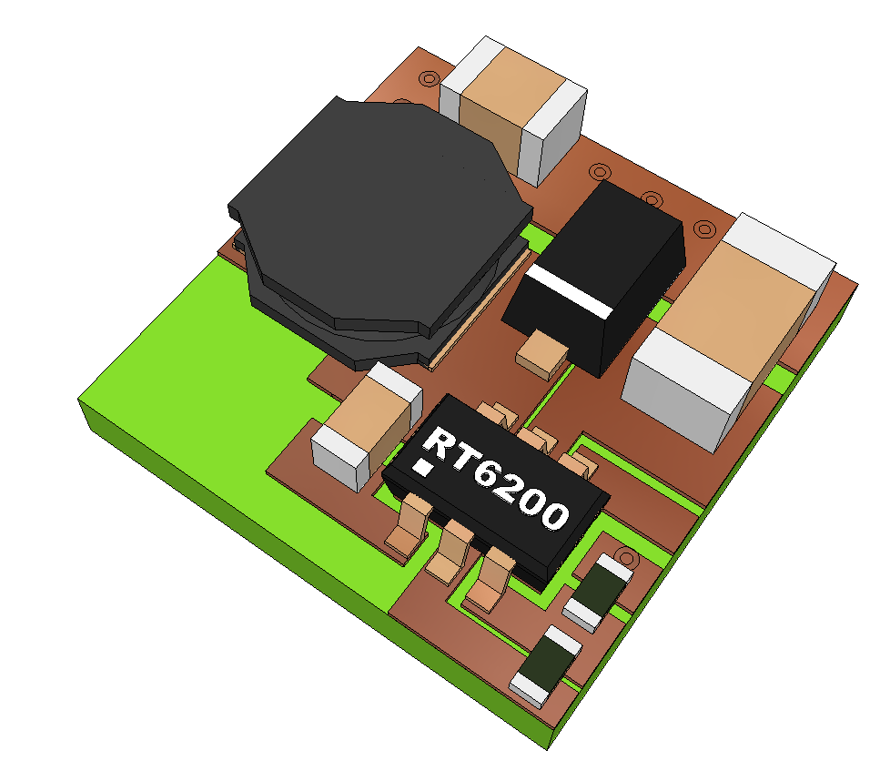
Figure 6.
4. RT6208 36V 0.1A High Efficiency Buck Converter
SoC parts with RF sections like Zigbee Light Link and Bluetooth Low Energy
have current consumption around 5 ~ 50mA. These SoC are often built into lighting
applications that run from higher voltage supply rails and need to achieve very
low total system standby power. They therefore need to achieve the highest possible
efficiency in the low current ranges. RT6208 was specially designed for these
types of applications, and minimizes converter losses by a special boundary
conduction mode / low quiescent current sleep mode cycling operation.
The RT6208 Block diagram and basic schematic are show in figure 7.
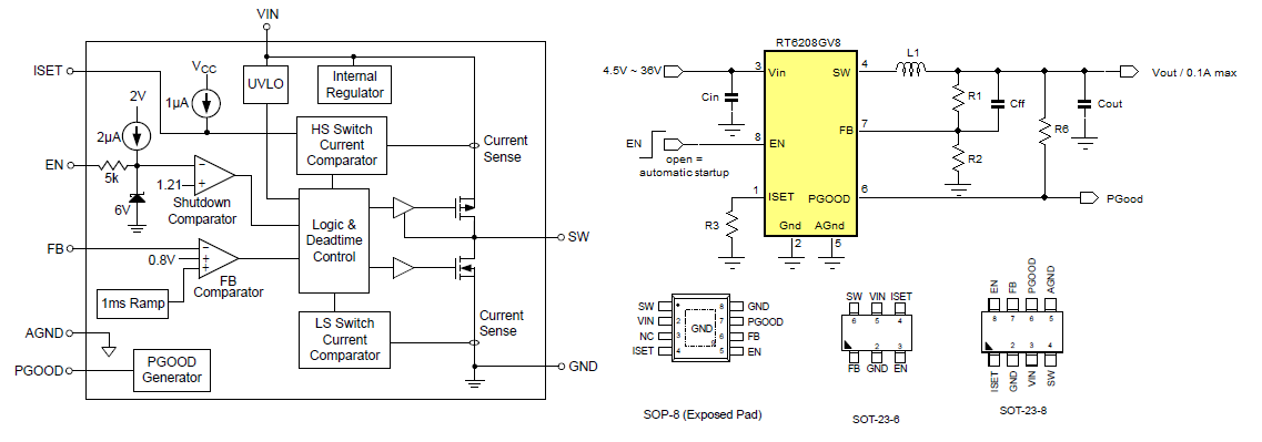
Figure 7.
The operation mode of RT6208 works as following: The external resistor on
the ISET pin sets an internal maximum peak current limit. The feedback comparator
has an 800mV reference and a 5mV hysteresis. When the feedback signal on FB
pin is 5mV lower than the internal reference, the internal high-side MOSFET
is switched on and inductor current begins to ramp up. When the inductor current
exceeds the internal peak current limit, the high-side MOSFET is switched off
and the low-side MOSFET is switched on. The inductor current ramps down to zero.
This triangular current pulse charges the output capacitor, and the FB pin rises
above the 800mV reference. After the inductor current reaches zero, both MOSFETs
are switched off and the converter is switched into a low quiescent current
sleep mode. The output voltage slowly discharges by the load current and when
the FB voltage drops 5mV below the reference, the high-side MOSFET is activated
again and the cycle repeats. In case of larger output capacitors or low current
limit settings, the converter will generate multiple switch cycles in boundary
conduction mode until the feedback pin exceeds the reference. This operation
minimizes switching losses, and achieves very good efficiency in light load
range.
Figure 8 below shows an application circuit for a for a 3.3V 50mA supply
with high efficiency at low current.
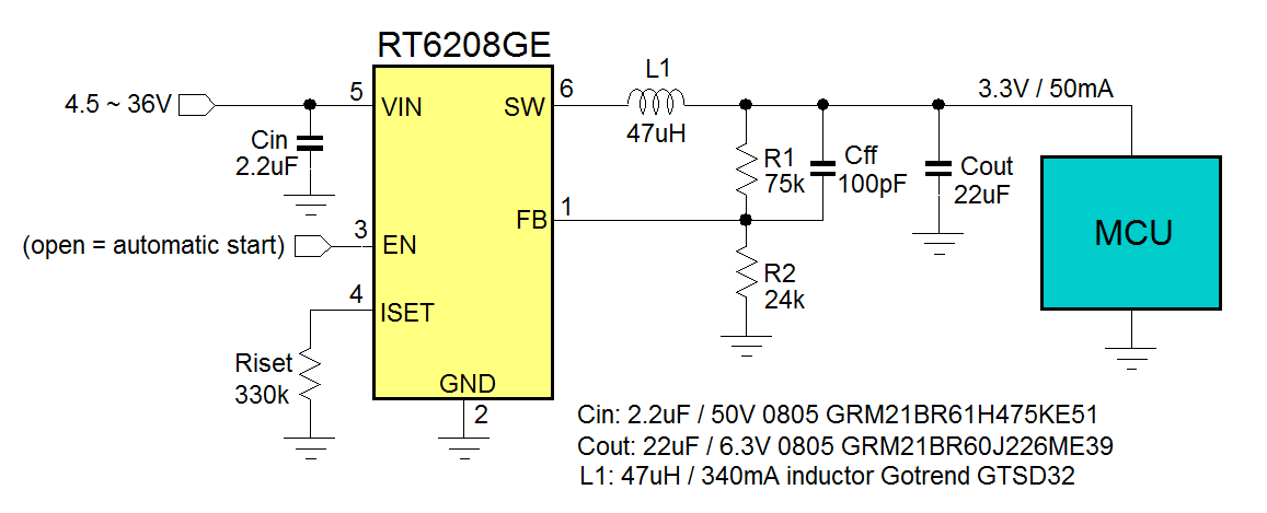
Figure 8.
The current limit setting determines the application maximum current and
should be chosen to be at least double the maximum load current: In this 50mA
maximum load example, RISET is calculated for a current limit of
106mA according:

This value sets the reference for the internal peak current sense comparator.
In practice, the actual peak current will be higher due to the peak current
level comparator propagation delay of ~100nsec. This increase in peak current
due to propagation delay depends on the dI/dt of the rising current slope, which
is dependent on Vin, Vout and L value. So high Vin applications with relatively
small inductors will show higher peak current than the programmed value.
Recommended inductor values for RT6208 3.3V and 5V applications range from
47 ~ 150µH. Larger inductor values reduce dI/dt, so application peak current
will be closer to the programmed value. Lower inductor values will result in
higher peak currents than programmed, but this does not impact overall performance.
Saturation current should be selected higher than the maximum application peak
current. In these low power applications, inductor core losses play an important
part in overall losses, and higher quality shielded inductors will have less
core losses than open semi-shielded types, thus improving efficiency.
RT6208 works in hysteretic output ripple based mode. The 5mV hysteresis at
the FB comparator means that the peak to peak output ripple will at least be
5mV * Vout/Vref. For calculating the output capacitor, the datasheet formula
provides a good guideline:
 This capacitor value will result in 1% output voltage ripple.
In the 3.3V example application using a 47µH inductor, a 106mA programmed
current will give around 200mA actual peak current at 24V input. The calculated
output capacitor value needs to be 8.6µF. A suitable choice is Murata
GRM21BR60J226ME39 22µF/6.3V 0805 which has around 9uF capacitance at 3.3V
due to DC bias and AC ripple effect.
To improve the switching stability of the hysteretic mode converter, a small
feed-forward capacitor Cff can be added in parallel with the upper feedback
resistor. This example uses 100pF.
For automatic start-up, the EN pin can be left floating.
Figure 9 below shows the output voltage, switching waveform and inductor
current at 5mA and 50mA load condition with different input voltages. It can
be seen that the inductor peak current increases with higher input voltages
due to comparator propagation delay. At 24V, one current pulse is sufficient
to produce an output ripple which can exceed the FB hysteresis. At 12V and higher
loads, two consecutive pulses are needed to exceed the FB hysteresis.
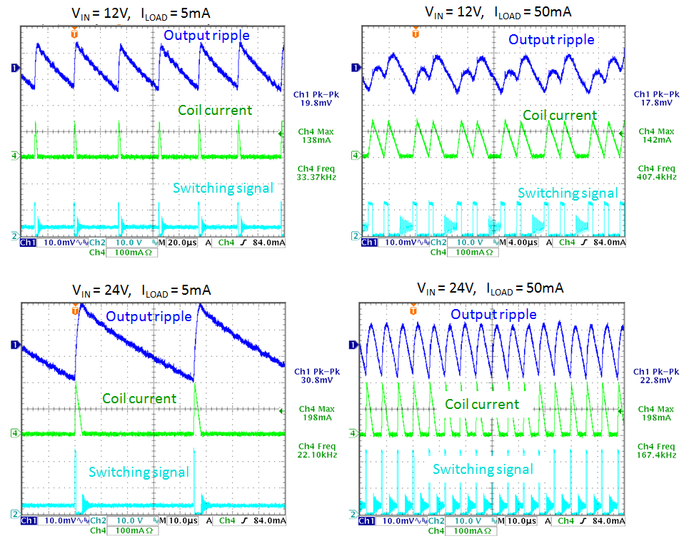
Figure 9.
The efficiency of the 24V – 3.3V / 50mA application is shown in figure
10. In the 5 ~ 50mA range, the efficiency is more than 80%, which helps to meet
low power standby requirements.
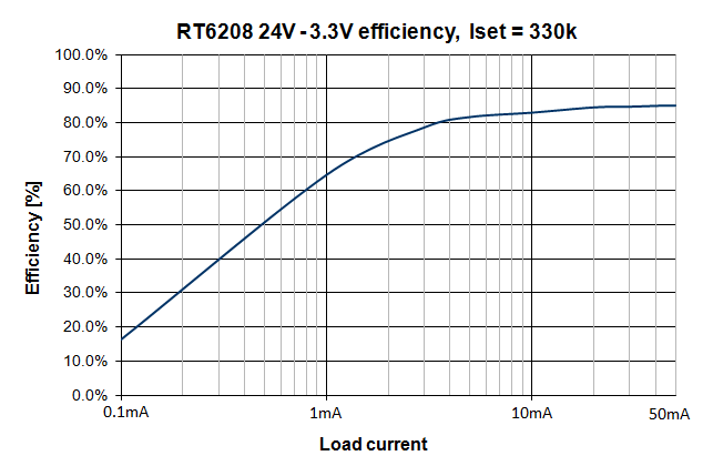
Figure 10.
An example layout is shown in figure 11. The power section is placed at the
left top corner, and several vias connect power ground to IC ground (underneath
the IC) via the inner ground layer. The feedback pin is sensitive to noise pick-up,
and the R1/R2 network should be placed close to this pin, away from noisy signals.
The ISET resistor is connected to the same small signal ground as the feedback
resistors. Total footprint of this layout is 7.5 x 8mm.
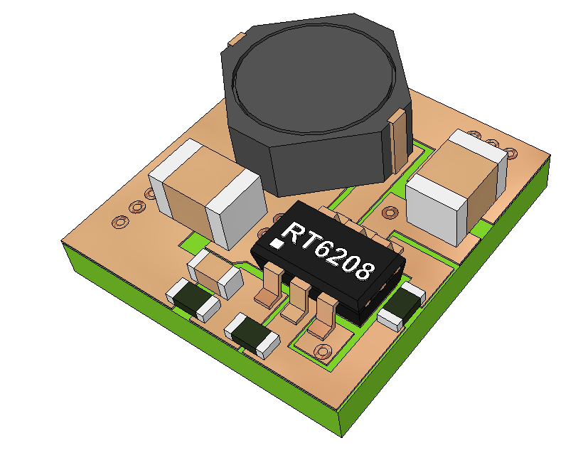
Figure 11.
5. Conclusion
In this application note two different methods are described to power microcontrollers
from 24Vinput voltage supplies: Linear regulators like RT9058, RT9069, RT9068
and RT9074 can be used when load current is small, up to 38mA depending on package.
For better efficiency and higher current levels, Buck converters like RT6200
and RT6208 can be used. RT6208 is especially suitable for applications that
require high efficiency at light loads.