General Description
The Evaluation Board demonstrates the RTQ5756A’s capability to be designed for a synchronous buck converter with 4-phase capability, allowing for both multiphase and single-phase operations. The RTQ5756A provides triple outputs with 2+1+1 phase. This flexibility and high integration make the RTQ5756 series suitable for various applications that require high current and compact power management solutions, such as low-power processors, I/O power, the core power of FPGAs, DSPs, and other ASICs. With an input voltage range of 3V to 5.5V, these converters are compatible with a wide variety of low voltage systems. They can deliver up to 10A peak current and support output voltages ranging from 0.4V to 2.05V.
The RTQ5756A offers programmable functions, including voltage level, voltage change slew rate, and soft-start slew rate, which can be controlled through an I2C interface operating at up to 3.4MHz. Additionally, the device also supports a remote-sense function to ensure accurate output voltage under heavy loads. It is equipped with interrupt and fault-detection functions to report any error status. The RTQ5756A is available in a WL-CSP-54B 2.69x3.92 (BSC) package.
Performance Specification Summary
Table 1 shows the summary of the RTQ5756A Evaluation Board performance specification. The ambient temperature is 25°C.
Table 1. RTQ5756A Evaluation Board Performance Specification Summary
|
Specification
|
Test Conditions
|
Min
|
Typ
|
Max
|
Unit
|
|
Input Voltage Range
|
|
3
|
--
|
5.5
|
V
|
|
Output Current
|
Vout1
|
0
|
--
|
10
|
A
|
|
Vout2, Vout3
|
0
|
--
|
5
|
A
|
|
Output Voltage Range
|
|
0.4
|
--
|
2.05
|
V
|
|
Operation Frequency
|
VOUT = 1V (FCCM)
|
--
|
2000
|
--
|
kHz
|
|
Output Ripple Voltage
|
VIN = 3.7V, VOUT = 1V
|
--
|
10
|
--
|
mVp-p
|
|
Line Regulation
|
3V £ VIN £ 5V, IOUT(DC) = 0A (FCCM)
|
--
|
0.2
|
--
|
%/V
|
|
Load Regulation
|
VIN = 3.7V, IOUT(DC) = 0A to 10A (FCCM)
|
--
|
-0.08
|
--
|
%/A
|
|
Load Transient Response
|
1-phase configuration, 0.01A to 2.5A,
tR = tF = 100ns, L= 0.22mH, VOUT = 1V,
COUT = 22mF x 2/phase, TA = 25°C (FCCM)
|
--
|
±50
|
--
|
mV
|
|
2-phase configuration, 0.01A to 5A,
tR = tF = 200ns, L= 0.22mH, VOUT = 1V,
COUT = 22mF x 2/phase, TA = 25°C (FCCM)
|
--
|
±50
|
--
|
mV
|
|
Maximum Efficiency
|
VIN = 3.3V, VOUT = 1V, IOUT = 1.6A
|
--
|
90.3
|
--
|
%
|
Power-Up Procedure
Suggestion Required Equipment
- RTQ5756A Evaluation Board
- DC power supply capable of at least 6V and 10A
- Electronic load capable of 10A
- Oscilloscope
- Richtek GUI tool
Quick Start Procedures
The Evaluation Board is fully assembled and tested. Follow the steps below to verify board operation. Do not turn on supplies until all connections are made. When measuring the output voltage ripple, care must be taken to avoid a long ground lead on the oscilloscope probe. Measure the output voltage ripple by touching the probe tip and ground ring directly across the last output capacitor.
Ensure proper measurement equipment setup, then follow the procedure below:
1. With power off, connect the input power supply to VIN and GND pins.
2. With power off, connect the electronic load between the VOUT1, VOUT2, VOUT3, and nearest GND pins.
3. With power off, connect the GUI tool to the computer through the USB port. Make sure the GUI software is installed on the computer, and the SDA (Serial Data), SCL (Serial Clock), and GND (Ground) signal wires from the Evaluation Board are connected to the corresponding ports on the GUI tool. Moreover, the VIO need to be powered by the same voltage level as SDA/SCL, which can be supplied by GUI tool 3.3V/1.8V.
4. Turn on the power supply at the input. Make sure that the input voltage does not exceed 6V on the Evaluation Board.
5. Use the RTQ5756A GUI to turn on the power rails by writing registers 0x49, 0x63, 0x7D bit0=1.
6. Check for the proper output voltage using a voltmeter.
7. Once the proper output voltage is established, adjust the load within the operating ranges and observe the output voltage regulation, ripple voltage, efficiency, and other performance.
Detailed Description of Hardware
Carefully inspect all the components used in the EVB according to the following Bill of Materials table, and then make sure all the components are undamaged and correctly installed. If there is any missing or damaged component, which may occur during transportation, please contact our distributors or e-mail us at evb_service@richtek.com.
Test Points
The EVB is provided with the test points and pin names listed in the table below.
|
Test Point/
Pin Name
|
Function
|
|
VIN
|
DC power supply positive input terminal. The input voltage range is from 3V to 5.5V after soft-start is finished.
|
|
VOUT1
|
Electronic load positive output terminal. Draw maximum output current up to 10A.
|
|
VOUT2
|
Electronic load positive output terminal. Draw maximum output current up to 5A.
|
|
VOUT3
|
Electronic load positive output terminal. Draw maximum output current up to 5A.
|
|
VIO
|
I/O supply voltage for digital communications. Connect this pin to 1.8V or 3.3V.
|
|
GND
|
Reference ground for power supply or electronic load. Provide the ground return path for the control circuitry and low-side power MOSFET.
|
|
SW_D
|
Switch node test point. The test point can be used to measure the SW_D signal.
|
|
SW_A
|
Switch node test point. The test point can be used to measure the SW_A signal.
|
|
SW_B
|
Switch node test point. The test point can be used to measure the SW_B signal.
|
|
SW_C
|
Switch node test point. The test point can be used to measure the SW_C signal.
|
|
EN
|
Enable control test point. The test point can be used to measure the EN signal.
|
|
INT
|
Interrupt indicator test point. The test point can be used to measure the INT signal.
|
|
WDOG_RST
|
Watchdog reset control input test point. The test point can be used to measure the WDOG_RST signal.
|
|
SDA
|
Data line for I2C interface test point. The test point can be used to measure the SDA signal.
|
|
SCL
|
Clock input for I2C interface test point. The test point can be used to measure the SCL signal.
|
|
VSEL1
|
Buck1 DVS register selection control input test point. The test point can be used to measure the VSEL1 signal.
|
|
VSEL2
|
Buck2 DVS register selection control input test point. The test point can be used to measure the VSEL2 signal.
|
|
VSEL3
|
Buck3 DVS register selection control input test point. The test point can be used to measure the VSEL3 signal.
|
|
VSEL4
|
Buck4 DVS register selection control input test point. The test point can be used to measure the VSEL4 signal.
|
|
JP1
|
EN jumper. Connect EN to logic-low to force the device into shutdown mode, connect logic-high to enable the converter.
|
|
JP2
|
INT jumper. Connect the INT pin to VIO with a pull-up resistor (R13) when the INT is set as open-drain type output. Leave the INT pin open when the INT is set as push-pull type output.
|
|
JP3
|
WDOG_RST jumper. Connect the WDOG_RST pin to the VIO pin voltage if this pin is not used.
|
|
JP4
|
I2C interface for Wrenboard or other GUI tools. Connect the SDA/SCL/GND signals to the corresponding ports on the GUI tool.
|
|
JP5
|
VSEL jumper. Connect the VSELx pin to the external control input or GPIOx from the GPIO jumper. Short the unused VSEL pin to GND.
|
|
JP6
|
VIO jumper. Connect VIO to VDDIO from the GUI tool. Leave the VIO pin open if VIO is supplied from an external source.
|
|
JP7
|
Mynaboard connector. It provides five GPIO control outputs, an I2C interface, and an IO voltage source adjusted by R21 and R22.
|
|
JP8
|
GPIO jumper. Use these five GPIO control outputs for VSEL and WDOG_RST control.
|
Software Installation
To use the Tool Kit (WrenBoard and Mynaboard) developed by Richtek, you must first install the required driver. Follow the steps below to complete the driver installation. Once the installation is finished, the GUI tool will be ready for use.
Step 1: After downloading the Richtek Bridgeboard Utilities, click on "Richtek Bridgeboard Utilities", and then click the "Install" button to begin the installation process, as shown in Figure 1.
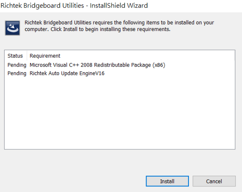
Figure 1. Driver Installation Step 1
Step 2: As shown in Figure 2, wait for the installation to proceed.
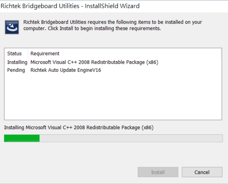
Figure 2. Driver Installation Step 2
Step 3: During the installation process, the window will appear, as shown in Figure 3. At this point, press the "YES" button to continue with the installation process.
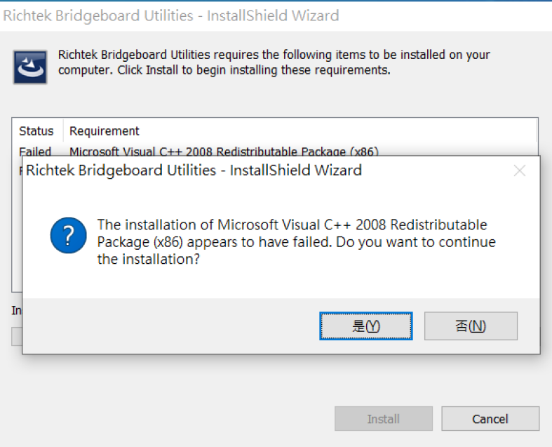
Figure 3. Driver Installation Step 3
Step 4: The installation will continue at this point. Wait for the installation process to proceed further, as shown in Figure 4.
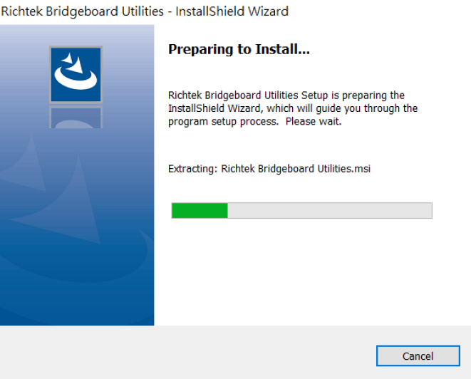
Figure 4. Driver Installation Step 4
Step 5 to 7: After clicking the "Next" button in Figure 5, the License Agreement screen will appear, as shown in
Figure 6. Choose to accept and continue by clicking the "Next" button. Then, after confirming the relevant information in Figure 7, click the "Next" button again to proceed.
Figure 5. Driver Installation Step 5
Figure 6. Driver Installation Step 6
Figure 7. Driver Installation Step 7
Step 8: In Figure 8, you can set the installation path. Once the path is set, click the "OK" button.
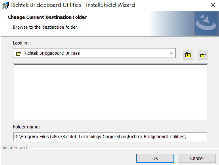
Figure 8. Driver Installation Step 8
Step 9: Figure 9 is a confirmation step to verify the installation path. If the information is correct, click the "Next" button to proceed with the rest of the installation.
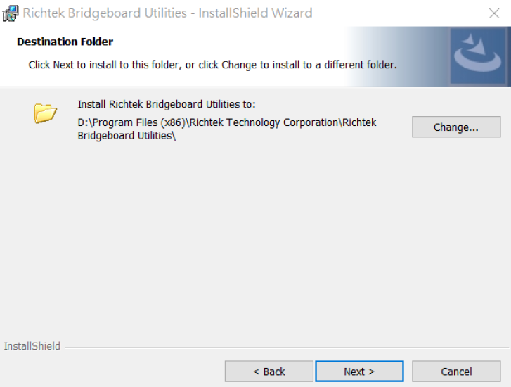
Figure 9. Driver Installation Step 9
Step 10 to 12: As shown in Figure 10, after confirming that all information is correct, click the "Install" button and wait for the installation progress bar to complete, as depicted in Figure 11. Once the installation is finished, click "Finish" to complete the entire driver installation process, as shown in Figure 12.
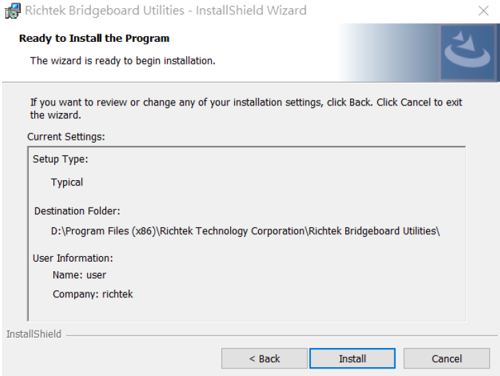
Figure 10. Driver Installation Step 10
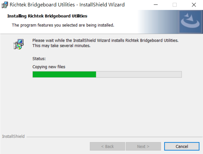
Figure 11. Driver Installation Step 11
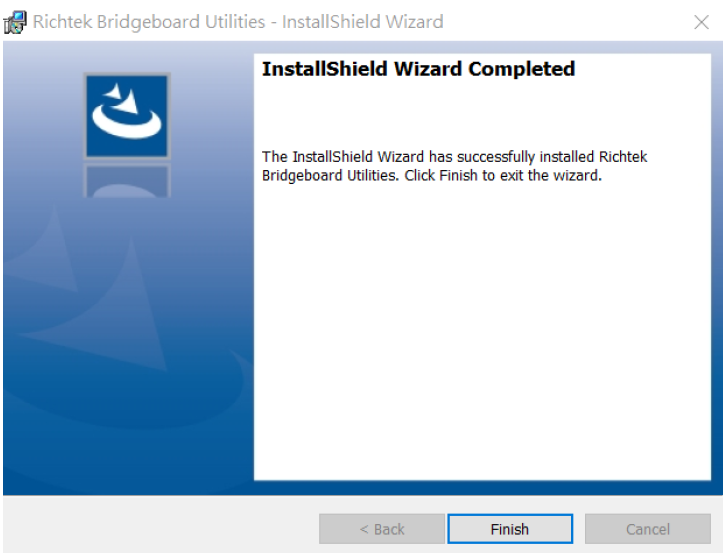
Figure 12. Driver Installation Step 12
Step 13: The RTQ5756_Setup_File for the RTQ5756A can be downloaded from the RTQ5756 official website under the Design Tools tab. After downloading, unzip the file and click the installer to begin the installation. Figure 13 demonstrates the installation process.
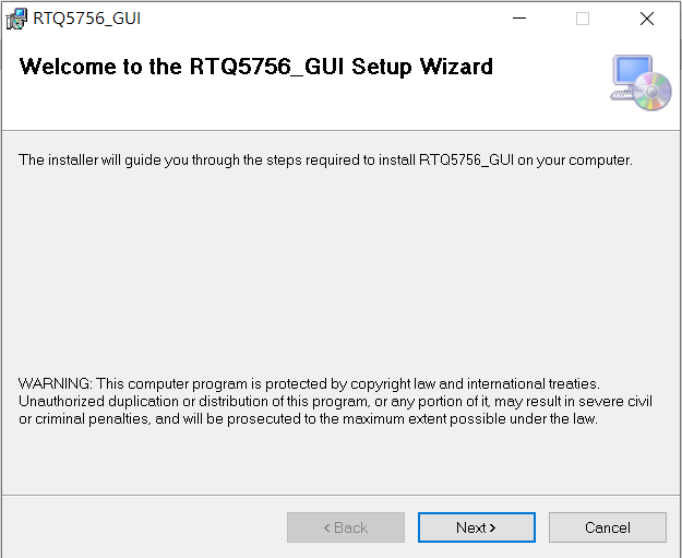
Figure 13. RTQ5756_GUI Installation Step 13
Step 14: During the installation process, set the installation path as needed, then continue with the installation until the software is completely installed. Once installation is complete, the RTQ5756_GUI can be used. Figure 14 shows the progress bar of the installation process.
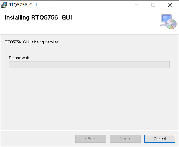
Figure 14. RTQ5756_GUI Installation Step 14
Graphical User Interface Overview
The RTQ5756A Evaluation Board includes the RTQ5756 GUI, which allows users to control the RTQ5756A.
Figure 15 shows the user-friendly Graphical User Interface.
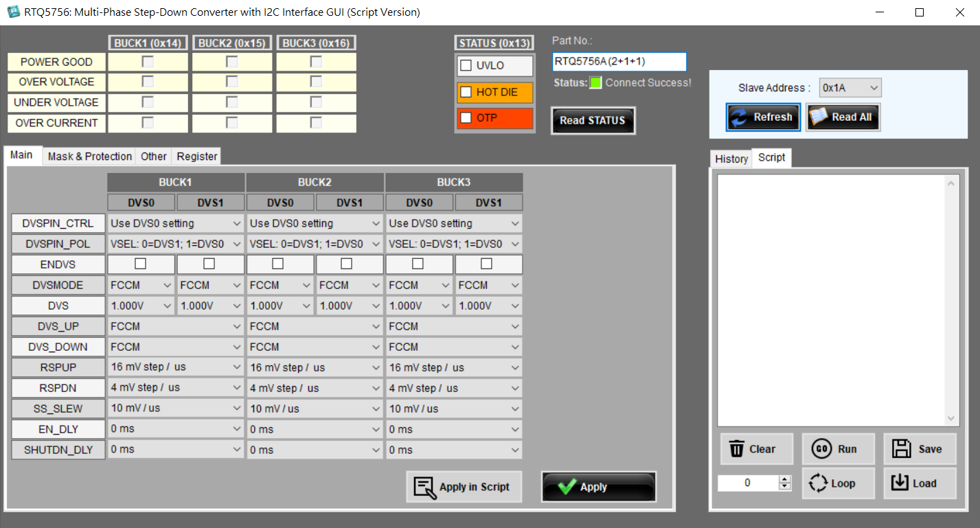
Figure 15. RTQ5756 Graphical User Interface
Quick Operation of the RTQ5756 EVB Software
The RTQ5756 GUI offers two methods for executing commands:
- Method 1: Direct command entry via the “Apply” button.
- Method 2: Write the desired commands in the “Script” window, and then press the “RUN” button.
Method 1: Direct command entry via the “Apply” button.
Step 1 to 4 introduce how to check the device connection, power on/off settings, output control settings, and other function setup. Users can easily complete the setup through direct command entry.
Step 1: Check the device connection status before getting start!
- Ensure that the Status shows green light and displays “Connect Success!”.
- Check the device “Slave Address” is right.
Step 2: Power on/off settings in the “Main” page
- Set the soft-start speed using “SS_SLEW” (options: 10,5,2.5,1.25 mV/us).
- Enable the device through the EN pin, and the delay time can be read from “EN_DLY” (range: from 0~63ms).
- Shut down through the EN pin, and the delay time can be set and read from “SHUTDN_DLY” (range: from 0~63ms).
Step 3: Output control settings in the “Main” page
- Set DVS control using “DVSPIN_CTRL” (use DVS0/DVS1/VSELx settings).
- Change the VSEL pin polarity through “DVSPIN_POL” (VSEL: 0=DVS0; 1=DVS1 or 0=DVS1; 1=DVS0).
- Enable or disable the power rail by checking the option “ENDVS” (DVS or DVS1: on/off).
- Select operation mode using “DVSMODE” (DVS0 or DVS1: FCCM/AUTO).
- Set dynamic voltage scaling via “DVS” (DVS or DVS1: 0.4V to 2.05V).
- Set DVS up mode using “DVS_UP” (FCCM/Auto mode).
- Set DVS down mode using “DVS_DOWN” (FCCM/Decay).
- Control DVS up and down speed control through “RSPUP” and “RSPDN” (16/8/4/2/1/0.5 mV/us).
Step 4: Other function setup in the “Mask & Protection” and “Other” pages
- Mask Power rail protection events: PG/OC/OV/UV/UVLO/Hot DIE/OT.
- Select Protection type for each power rail: UV Hiccup/UV Shutdown.
- Set INT pin CMOS type: Open drain/sourcing and sinking (push-pull).
- Configure INT pin INVERT option: Active low/active high.
- Select Watchdog reset power rail: Buck1/Buck2/Buck3.
- Set Watchdog reset delay time: 0/1.56/3.125/6.25/12.5/9/15.25/14.5ms.
- Reset all registers to default values.
Method 2: Write the desired commands in the “Script” window, and then press the “RUN” button.
The following methods show how to implement power on/off sequence control to achieve 100us delay between Buck1 and Buck2, and 200us delay between Buck2 and Buck3 via the “Script” function, which is only supported by the Richtek GUI tool “Mynaboard”.
Perform the power on through the I2C command in Script
Line 1: W 0x49 0x21
Line 2: Delay (0.1)
Line 3: W 0x63 0x21
Line 4: Delay (0.2)
Line 5: W 0x7D 0x21
Perform the power on through the VSEL pin
Set the DVS control to VSELx, and make sure the VSEL polarity meet the I/O control requirements. The Richtek GUI tool “Mynaboard” offers five GPIO ports for users to control the I/O pin. The RTQ5756A possesses three VSEL pins (VSEL1/2/3), which can be controlled by GPIO1/2/3, respectively. The commands are shown as follows:
Line 1: GPIO (1) (High)
Line 2: Delay (0.1)
Line 3: GPIO (2) (High)
Line 4: Delay (0.2)
Line 5: GPIO (3) (High)
Bill of Materials
|
Reference
|
Count
|
Part Number
|
Value
|
Description
|
Package
|
Manufacturer
|
|
U1
|
1
|
RTQ5756AWSC-00
|
2+1+1 configuration
|
Buck Converter
|
WL-CSP-54B 2.69x3.92 (BSC)
|
RICHTEK
|
|
C1, C2, C3
|
3
|
GRM31CE70J476ME15L
|
47μF
|
Capacitor, Ceramic, 6.3V, X7U
|
1206
|
MURATA
|
|
C4,C6,C8,C10
|
4
|
GRM188D70J106MA73D
|
10μF
|
Capacitor, Ceramic, 6.3V, X7T
|
0603
|
MURATA
|
|
C5,C7,C9,C11,C16,C21,C26,C31
|
8
|
0402B104K500CT
|
0.1μF
|
Capacitor, Ceramic, 50V, X7R
|
0402
|
WALSIN
|
|
C12,C13,C17,
C18,C22,C23,
C27,C28
|
8
|
GRM188C80G226ME15D
|
22μF
|
Capacitor, Ceramic, 4V, X6S
|
0603
|
MURATA
|
|
C32,C33
|
2
|
GRM155C71C105KE11D
|
1μF
|
Capacitor, Ceramic, 16V, X7S
|
0402
|
MURATA
|
|
L1,L2,L3,L4
|
4
|
HMMQ25201B-R22MSR
|
0.22μH
|
Inductor, Isat=7.7A, DCR=8mΩ
|
2.5x2.0x1.2 mm3
|
CYNTEC
|
|
R1,R2,R3,R5,R6,R8,R10,R11,
R12,R15,R16
|
11
|
WR06X000 PTL
|
0
|
Resistor, Chip, 1/10W
|
0603
|
WALSIN
|
|
R13,R14,R22
|
3
|
WR06X1002FTL
|
10k
|
Resistor, Chip, 1/10W, 1%
|
0603
|
WALSIN
|
|
R21
|
1
|
WR06X1001FTL
|
1k
|
Resistor, Chip, 1/10W, 1%
|
0603
|
WALSIN
|
Typical Applications
EVB Schematic Diagram
1. The capacitance values of the input and output capacitors will influence the input and output voltage ripple.
2. MLCC capacitors have degrading capacitance at DC bias voltage, and especially smaller size MLCC capacitors will have much lower capacitance.
Measure Result
|
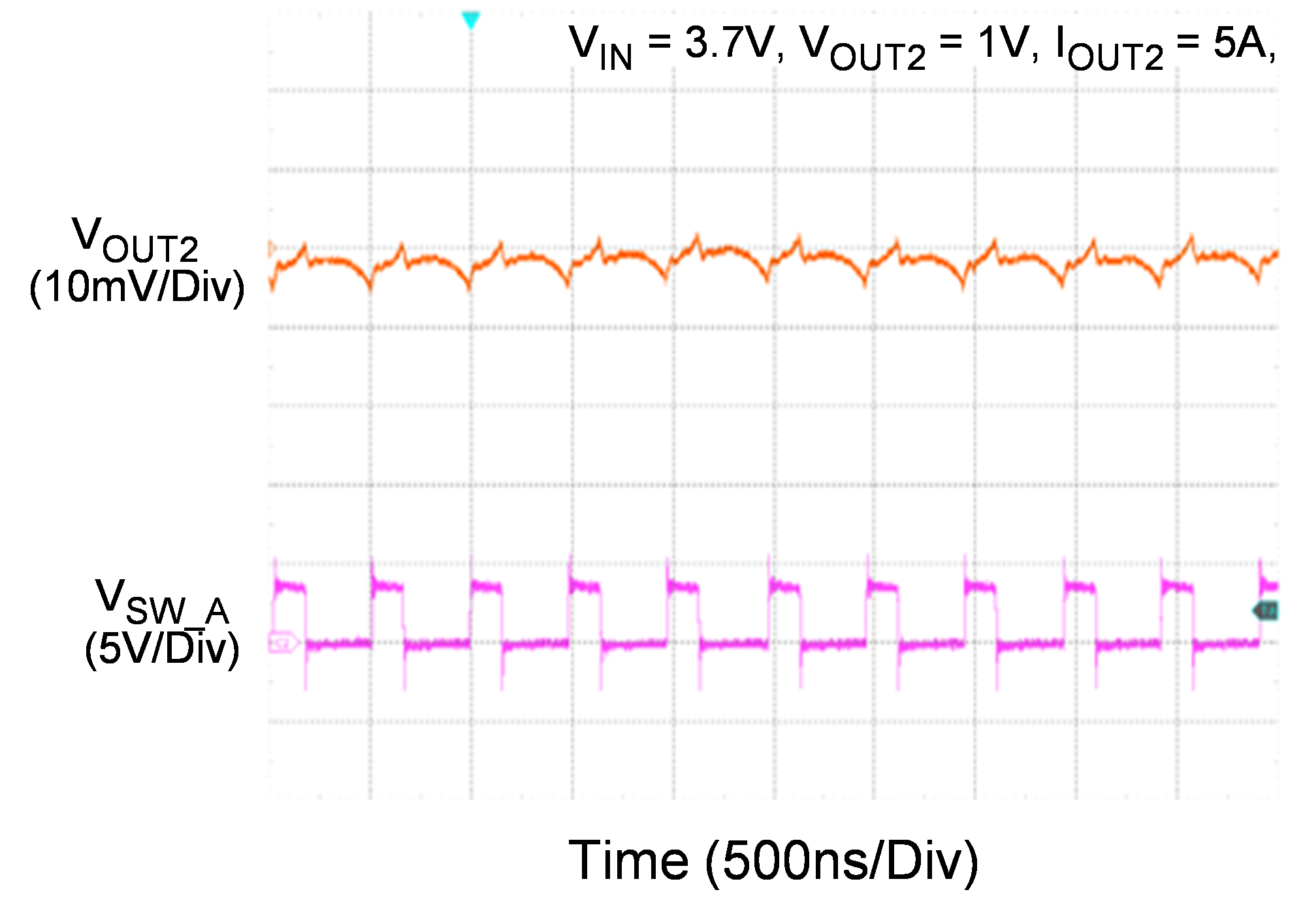
Output Ripple Voltage
|
Output Ripple Voltage
|
|
|
|
|
Output Ripple Voltage
|
Output Ripple Voltage
|
|
|
|
|
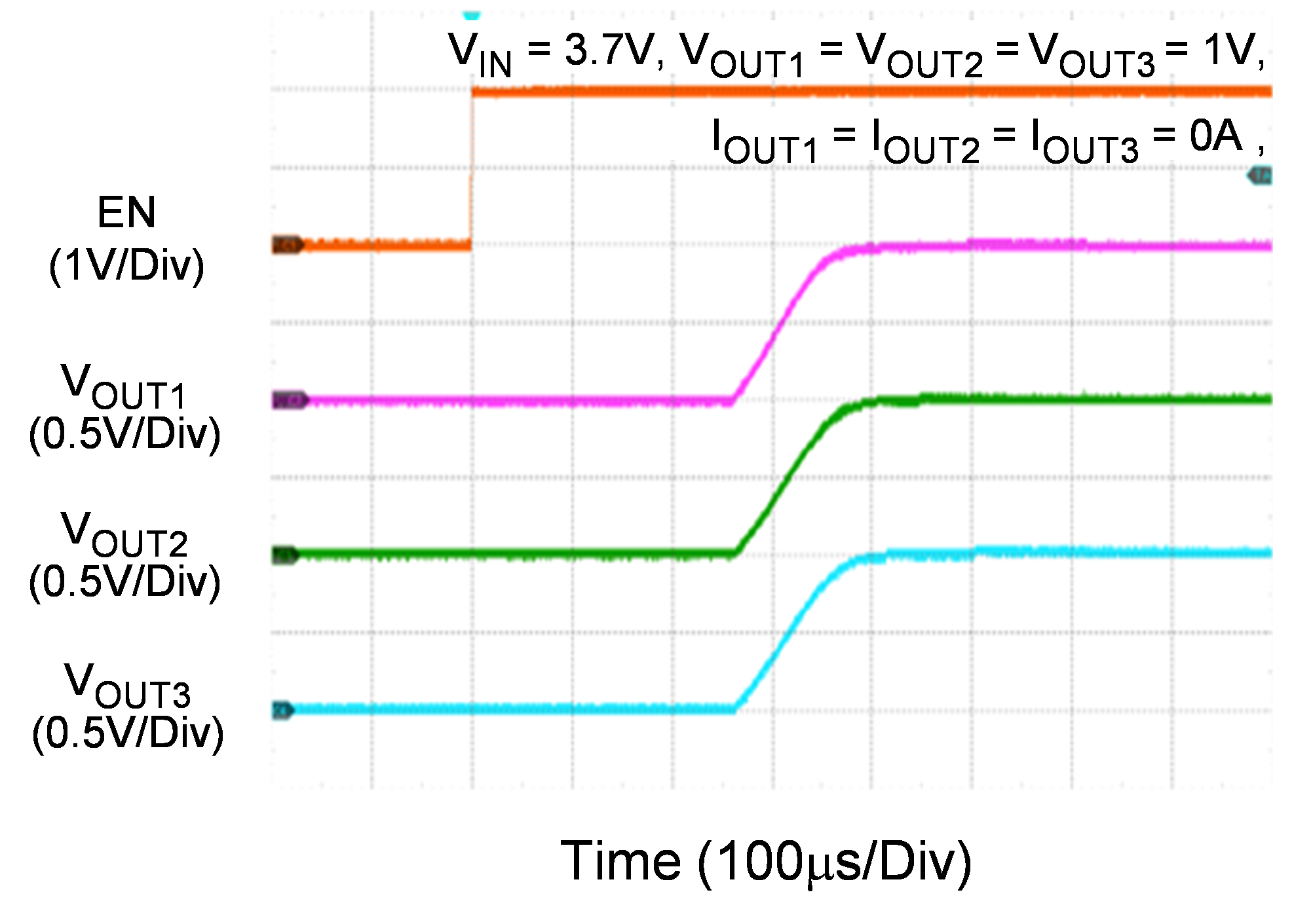
Power On from EN
|
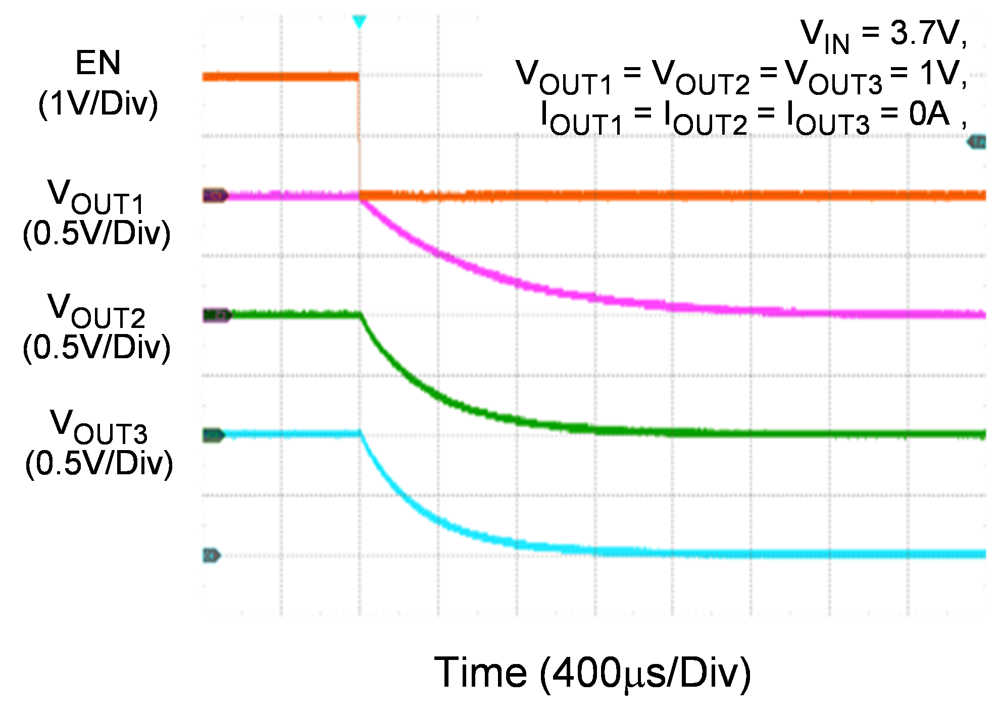
Power Off from EN
|
|
|
|
|
Power On from SW EN
|
Power Off from SW EN
|
|
|
|
|
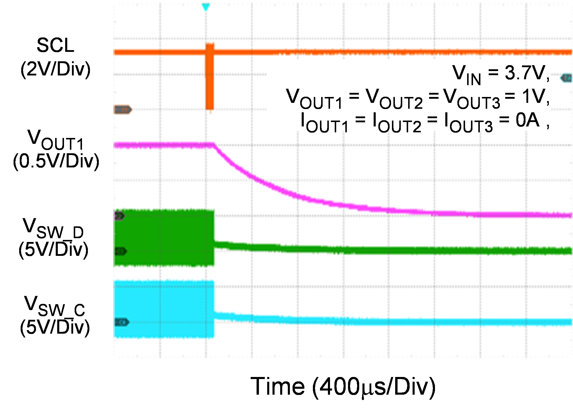
Short Circuit Response with VOUT1 Short to GND – Hiccup Mode
|
Short Circuit Response with VOUT1 Short to GND – Latch Mode
|
|
|
|
|
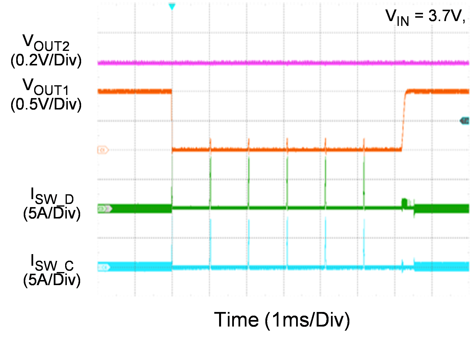
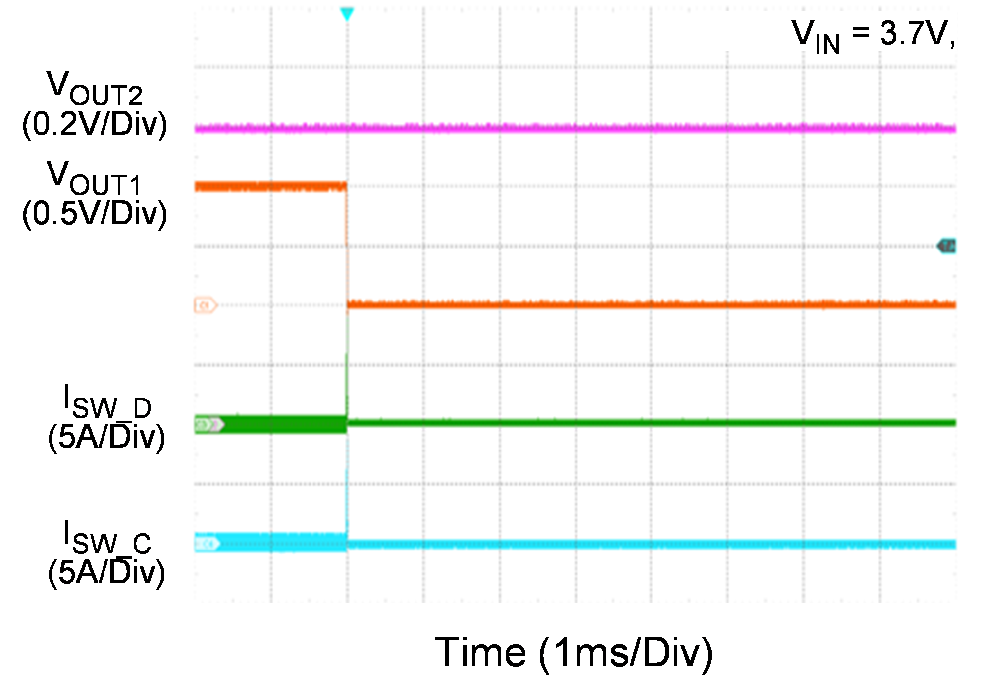
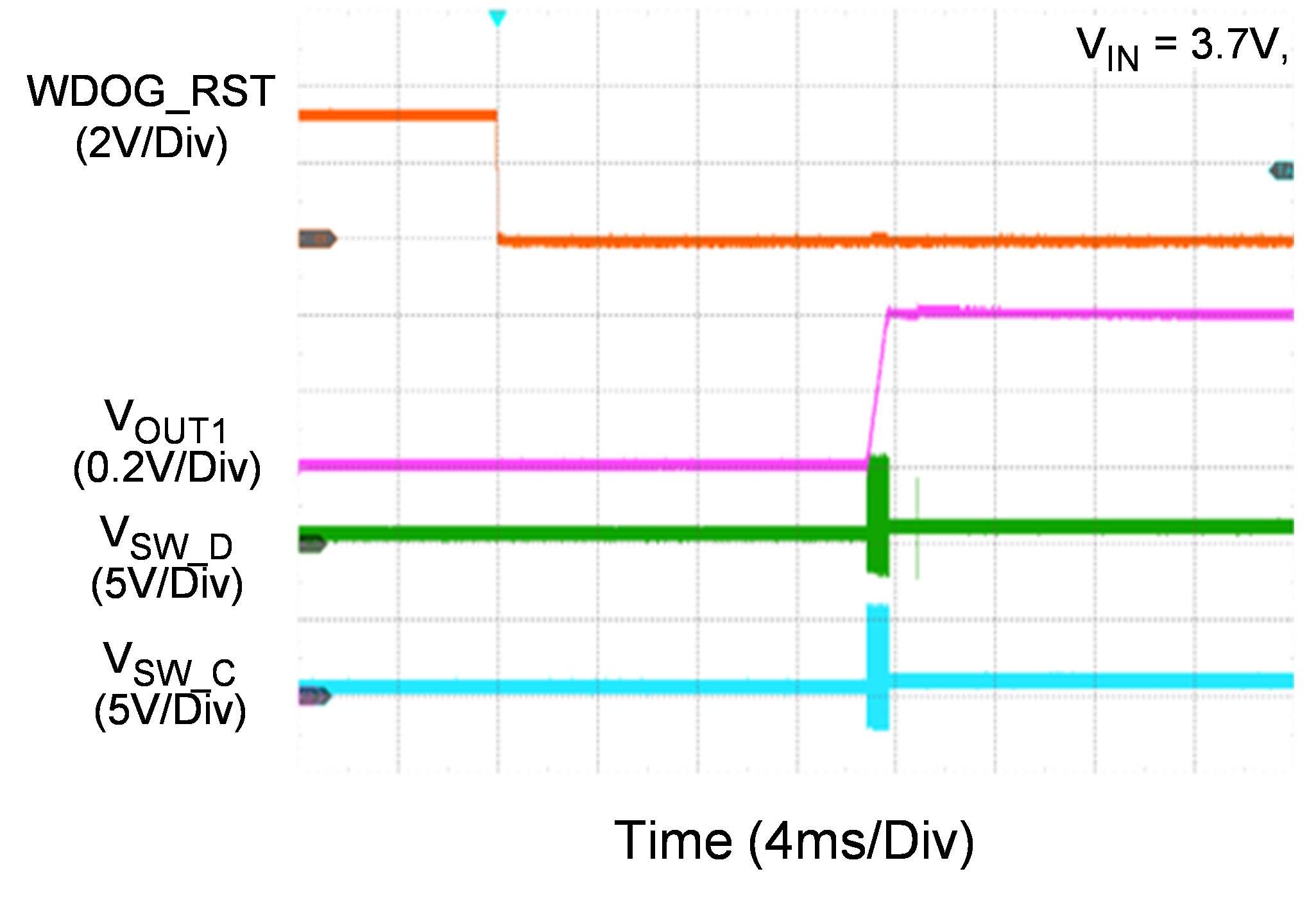
Watchdog Reset Function with 0ms delay
|
Watchdog Reset Function with 15.25ms delay
|
|
|
|
|
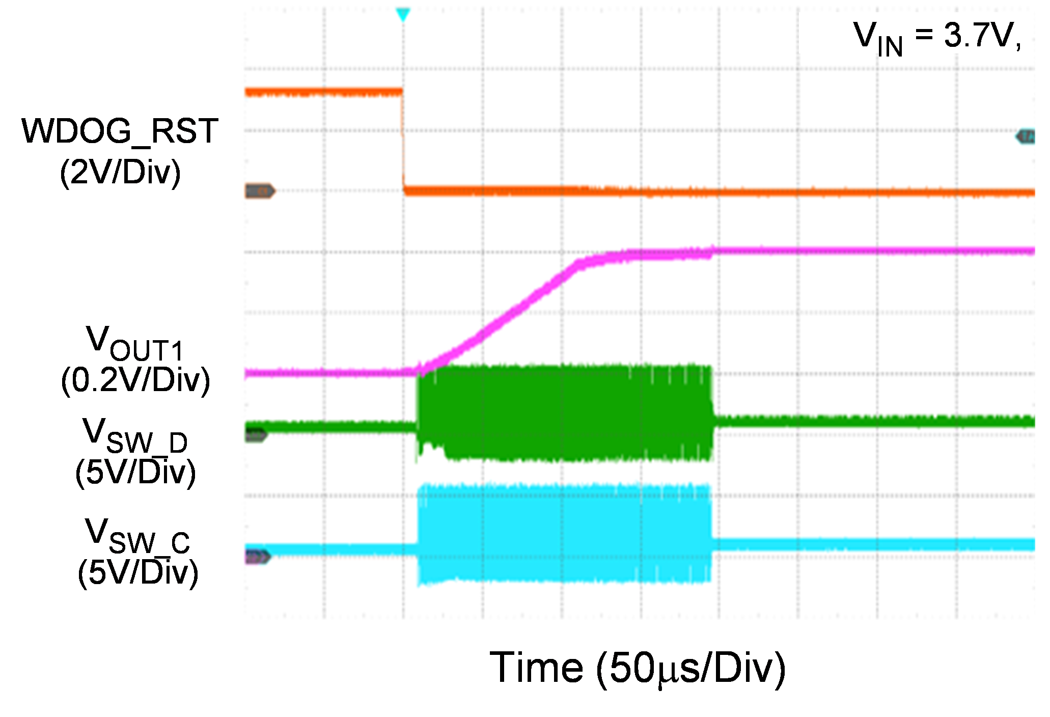
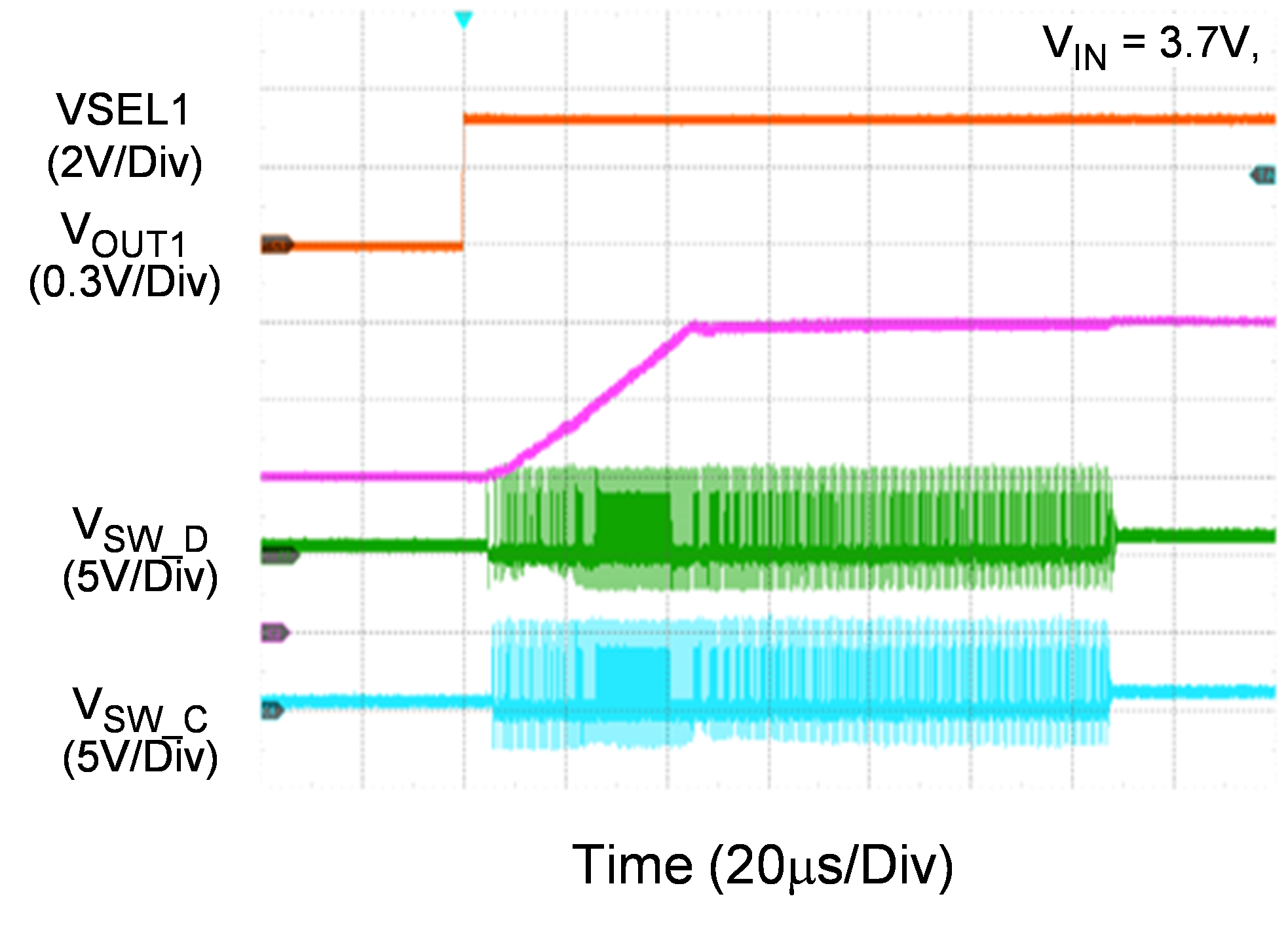
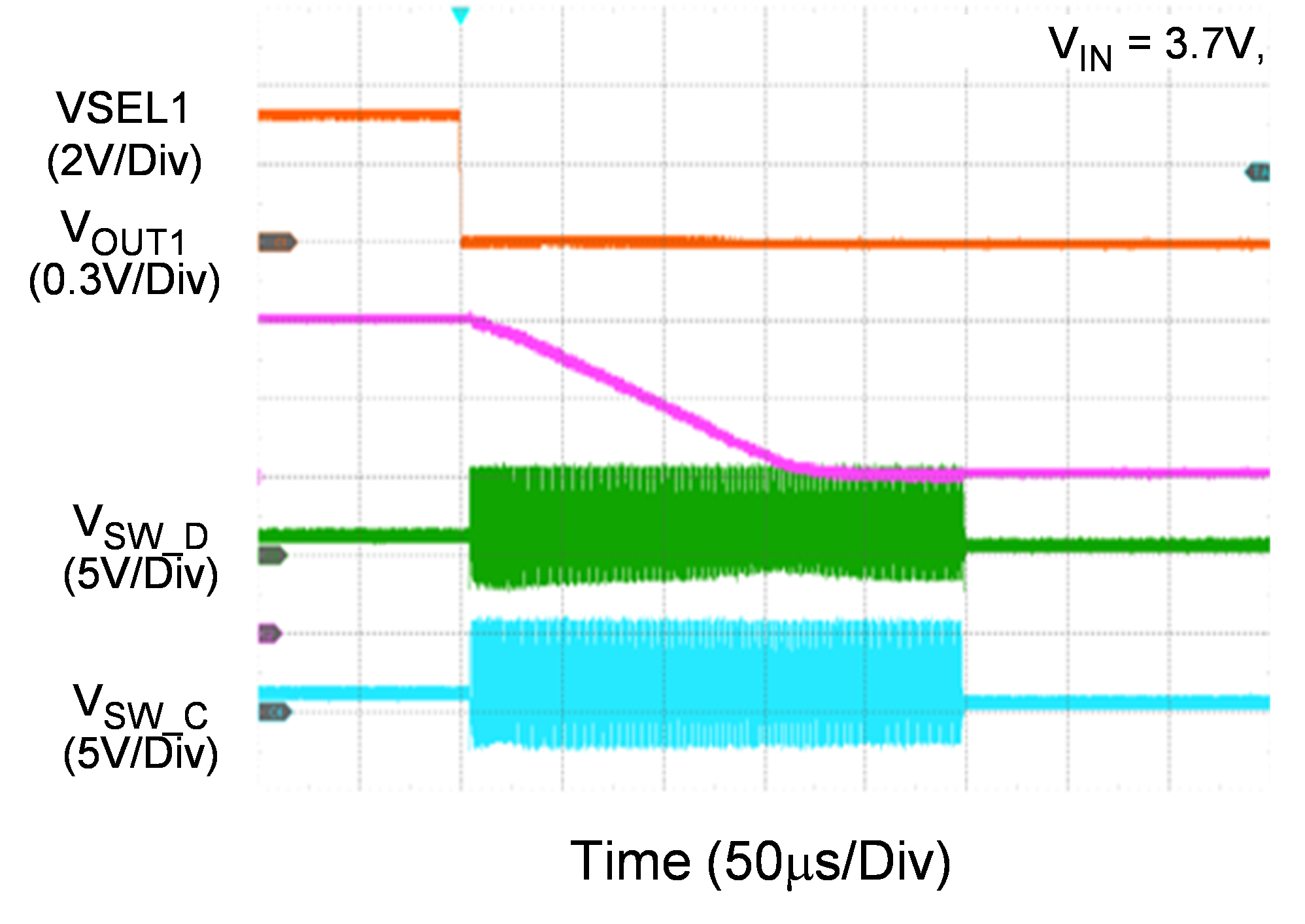
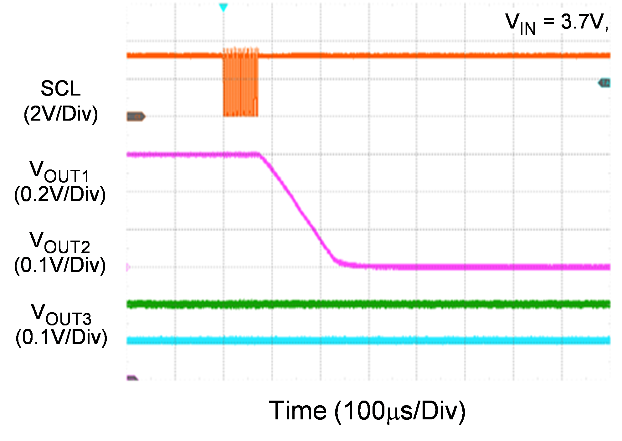
Dynamic Voltage Scaling with VSEL1 Control
|
Dynamic Voltage Scaling with VSEL1 Control
|
|
|
|
|
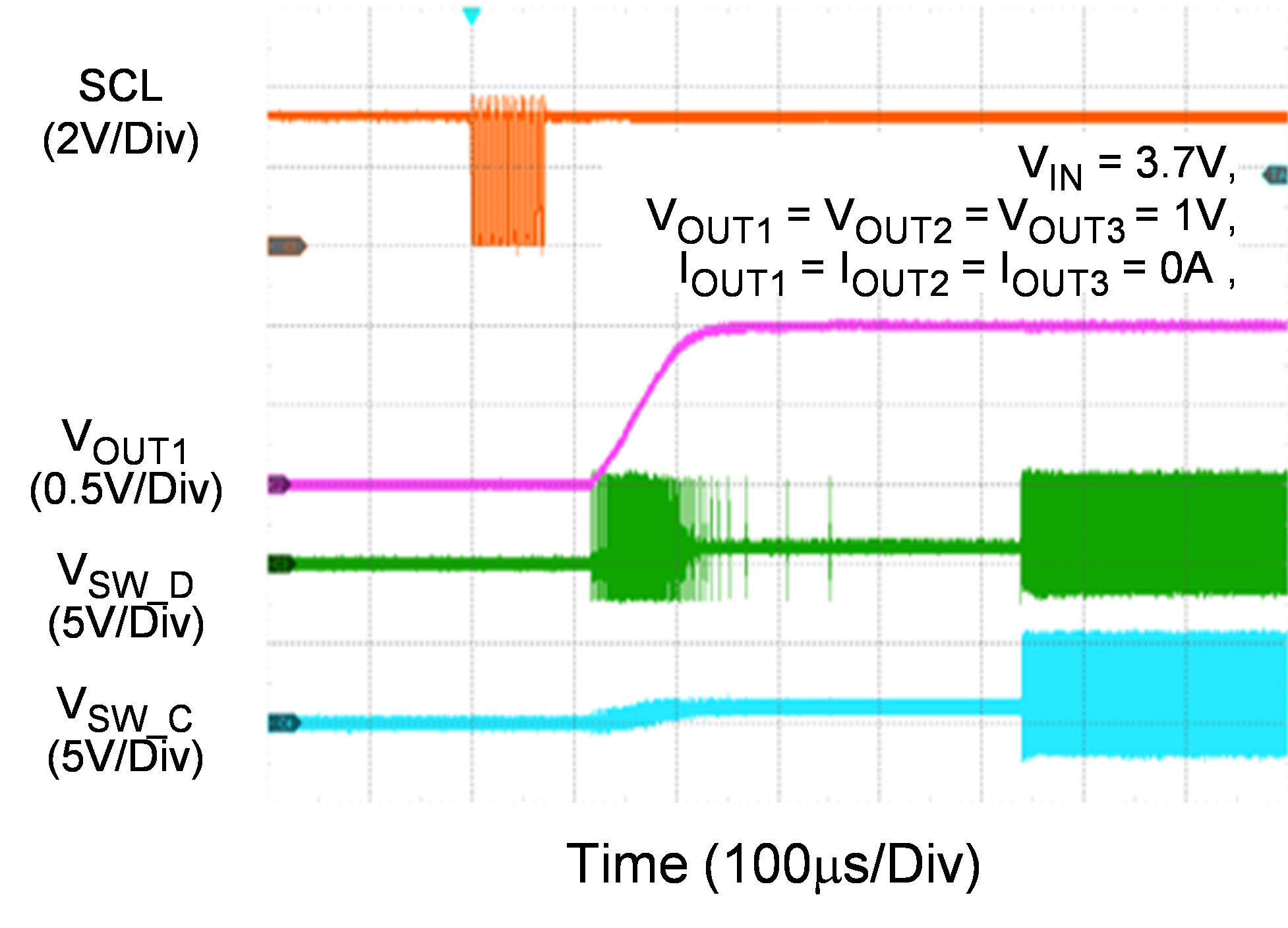
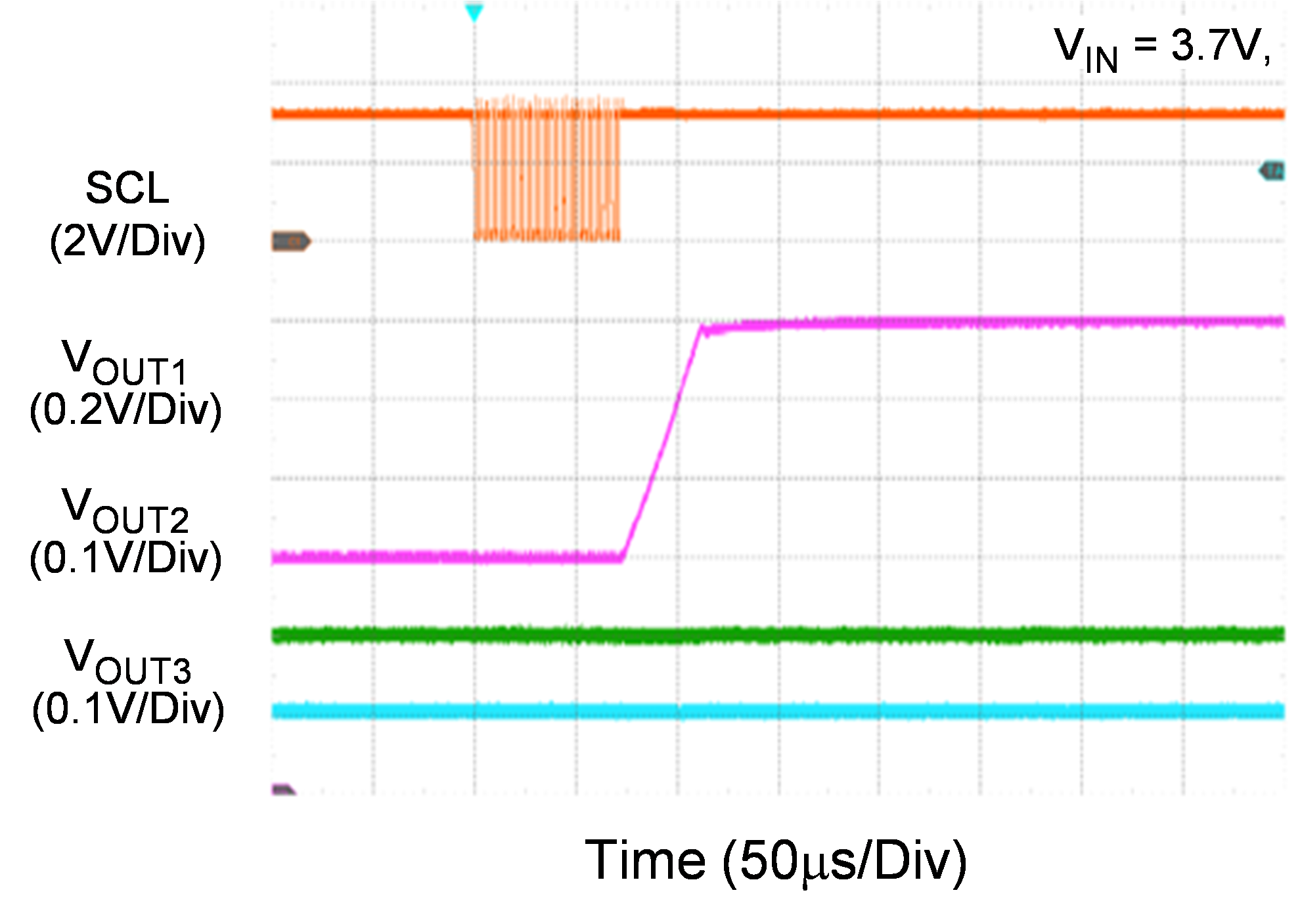
Dynamic Voltage Scaling with I2C Control
|
Dynamic Voltage Scaling with I2C Control
|
|
|
|
|
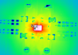
Thermal Image at VIN = 3.3V, VOUT1 = VOUT2 = VOUT3 =1V, IOUT1 = 5A, IOUT2 = IOUT3 =2.5A
|
|
|
Note: When measuring the input or output voltage ripple, care must be taken to avoid a long ground lead on the oscilloscope probe. Measure the output voltage ripple by touching the probe tip directly across the output capacitor.
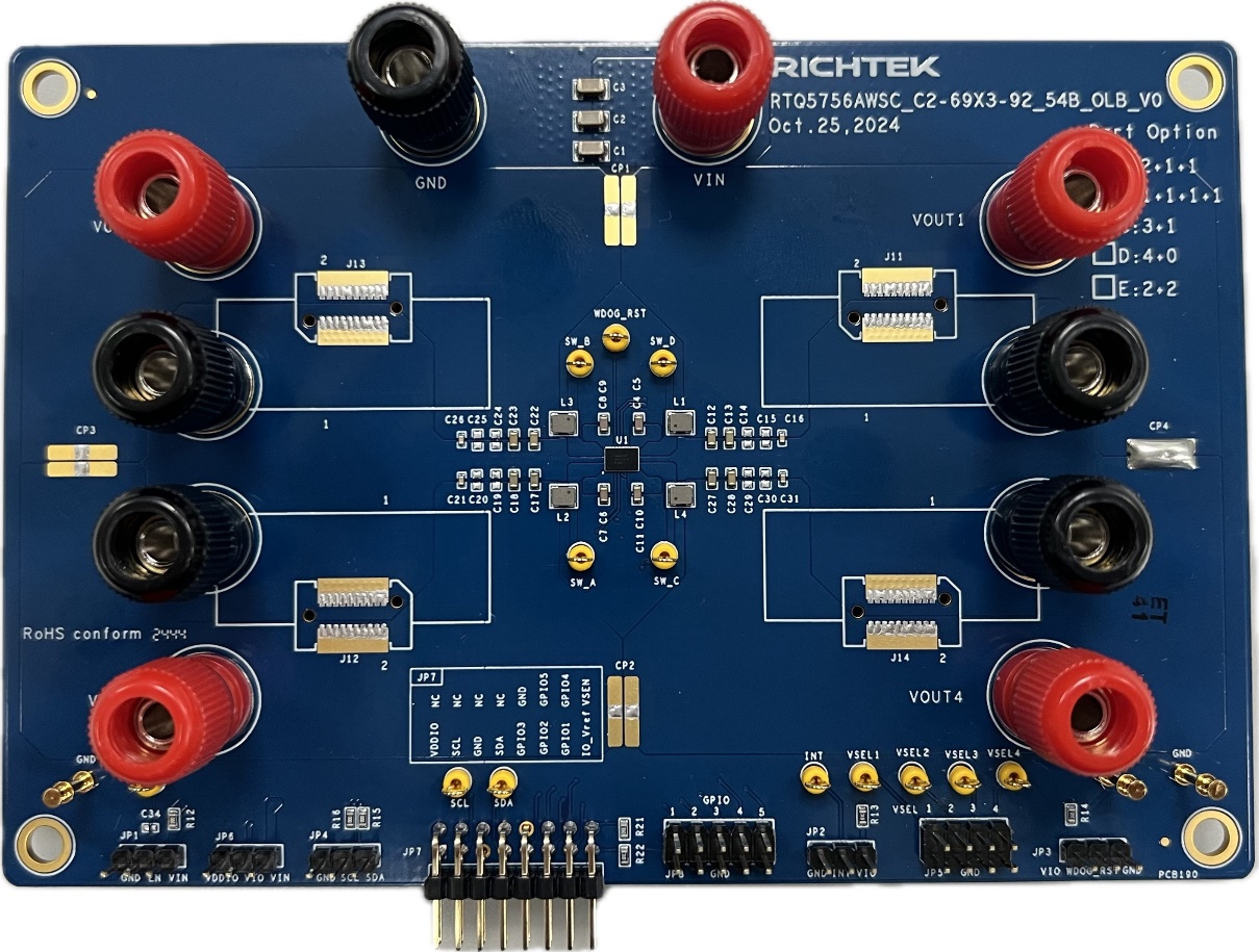
Evaluation Board Layout
Figure 1 to Figure 4 show the layout of the RTQ5756 Evaluation Board. This board size is 147mm x 100mm and is constructed on four-layer PCB, outer layers with 1 oz. Cu, and inner layers with 1 oz. Cu.
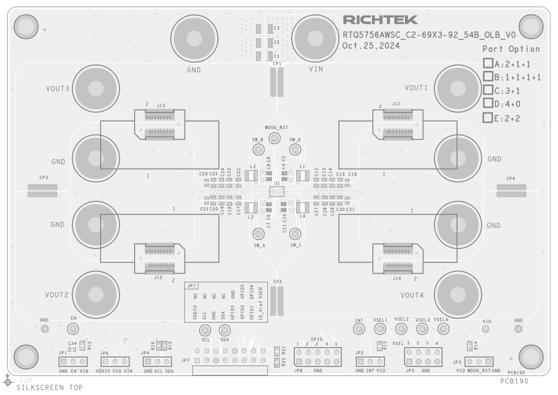
Figure 1. Top View (1st layer)
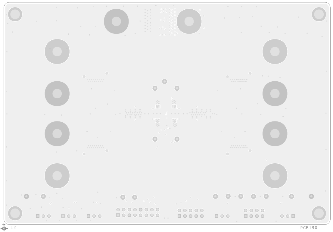
Figure 2. PCB Layout—Inner Side (2nd Layer)
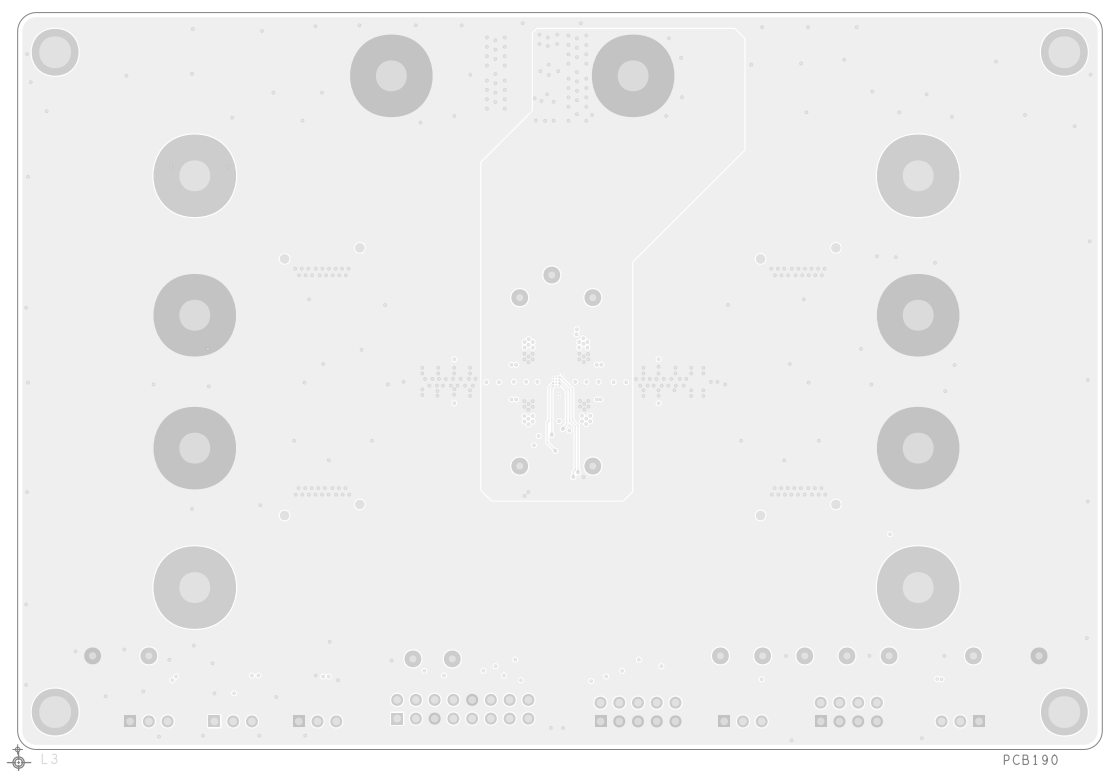
Figure 3. PCB Layout—Inner Side (3rd Layer)
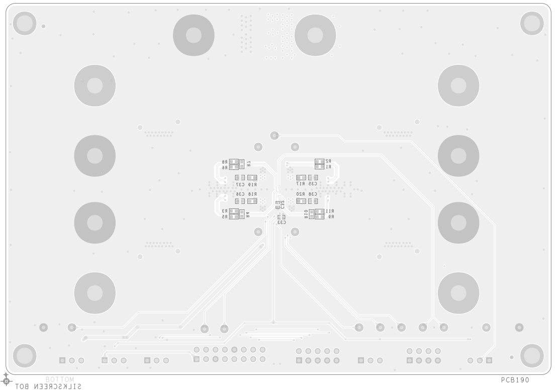
Figure 4. Bottom View (4th Layer)