General Description
The RT6166D is a high-efficiency, single-inductor, Advanced Constant On-Time (ACOT®) monolithic synchronous buck-boost converter that can deliver up to 3A output current from a 2V to 5.5V input supply. It provides precise regulation to the digitally programmable output voltage from 1.8V to 4.975V, making it suitable for wide input supply range applications, regardless of whether the input voltage is lower than, higher than, higher than, or equal to the output voltage. This document explains the function and use of the RT6166D evaluation board (EVB), and provides information related to the configuration and settings of the evaluation board.
Performance Specification Summary
Table 1 shows the summary of the RT6166D Evaluation Board performance specification. The ambient temperature is 25°C.
Table 1. RT6166D Evaluation Board Performance Specification Summary
|
Specification
|
Test Conditions
|
Min
|
Typ
|
Max
|
Unit
|
|
Input Voltage Range
|
|
2
|
--
|
5.5
|
V
|
|
Output Current
|
VIN ≥ 2.5V, VOUT = 3.3V
|
0
|
--
|
2.5
|
A
|
|
VIN ≥ 3V, VOUT = 3.3V
|
0
|
--
|
3
|
|
Output Voltage Range
|
|
1.8
|
--
|
4.975
|
V
|
|
Switching Frequency
|
|
--
|
2.2
|
--
|
MHz
|
|
IQ_SW
|
VEN = VIN = 3.6V, IOUT = 0A
|
--
|
4
|
7
|
µA
|
|
IQ_NON-SW
|
VEN = VIN = 3.6V, IOUT = 0A, not switching
|
--
|
3
|
5
|
|
ISHDN
|
VEN = 0V, VIN = 3.6V
|
--
|
1
|
2
|
µA
|
Power-Up Procedure
Suggestion Required Equipment
- RT6166D Evaluation Board
- DC power supply capable of at least 5.5V and 7A
- Electronic load capable of 10A
- Function Generator
- Oscilloscope
Quick Start Procedures
The Evaluation Board is fully assembled and tested. Follow the steps below to verify board operation. Do not turn on supplies until all connections are made. When measuring the output voltage ripple, care must be taken to avoid a long ground lead on the oscilloscope probe. Measure the output voltage ripple by touching the probe tip and ground ring directly across the last output capacitor.
Proper measurement equipment setup and follow the procedure below.
1) Output selection: the RT6166D has external VSEL pin to select VOUT1 or VOUT2. Pulling VSEL to high is for VOUT2 and pulling VSEL to low is for VOUT1.
2) VOUT selection: the RT6166D has a programmable VOUTX [6:0] register, allowing output voltage adjustment from 1.8V to 4.975V with 25mV resolution per step. The VOUT1 Address = 0x04 and VOUT2 Address = 0x05
3) With power off, connect the input power supply to the VIN and GND pins.
4) With power off, connect the electronic load between the VOUT pin and the nearest GND pin.
5) Turn on the power supply at the input. Make sure that the input voltage does not exceed 5.5V on the evaluation board.
6) Pull the RT6166D En pin high to enable device, that is, switching being enabled and soft-start sequence being initiated. It is recommended that the VIN voltage is higher than VUVLO first, then the EN voltage rises above the logic-high threshold voltage (VENH), the device will be turned on.
7) To verify the output voltage VOUT. If VSEL = H, default output voltage of RT6166D measurement is 3.45V; If VSEL = L, default output voltage of RT6166D measurement is 3.85 V. Check for the proper output voltage using a voltmeter.
8) Once the proper output voltage is established, adjust the load within the operating ranges and observe the output voltage regulation, ripple voltage, efficiency, and other performance.
Detailed Description of Hardware
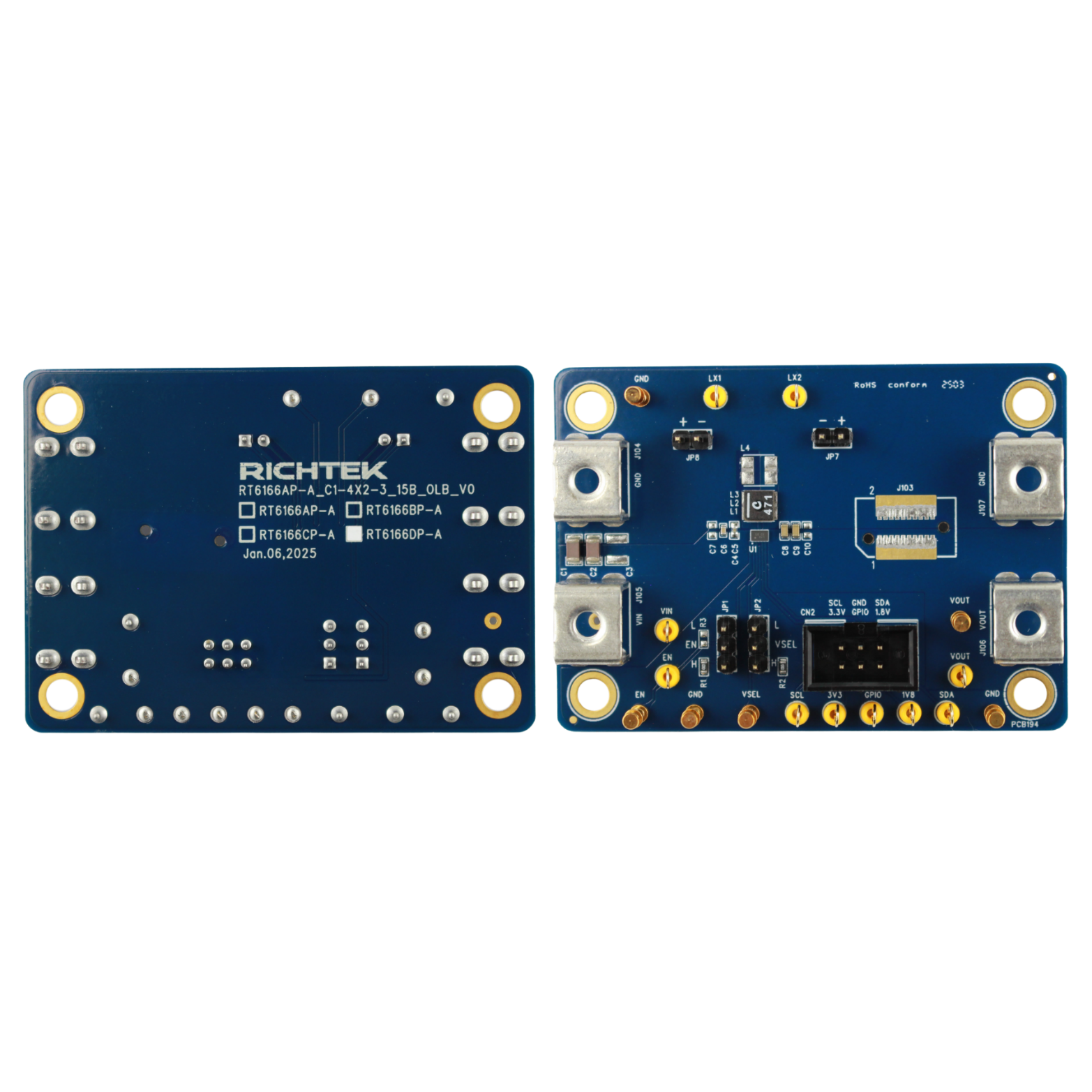
Carefully inspect all the components used in the EVB according to the following Bill of Materials table, and then make sure all the components are undamaged and correctly installed. If there is any missing or damaged component, which may occur during transportation, please contact our distributors or e-mail us at evb_service@richtek.com.
Test Points
The EVB is provided with the test points and pin names listed in the table below.
|
Test Point / Pin Name
|
Function
|
|
VIN
|
Input voltage.
|
|
VOUT
|
Output voltage.
|
|
GND
|
Ground.
|
|
EN
|
Enable test point.
|
|
LX1
|
Switching node1 of LX
|
|
LX2
|
Switching node2 of LX
|
|
VSEL
|
Output voltage selection pin.
|
Bill of Materials
|
Reference
|
Count
|
Part Number
|
Value
|
Description
|
Package
|
Manufacturer
|
|
U1
|
1
|
RT6166DP-A
|
RT6166DP-A
|
Buck-Boost Converter
|
WL-CSP-15B 1.4x2.3
|
RICHTEK
|
|
C1, C2
|
2
|
GRM31CR71A226KE15
|
22µF
|
22µF/16V/X5R
|
1206
|
Murata
|
|
C4
|
1
|
GRM033R60J104KE19D
|
100nF
|
100nF/6.3V/X5R
|
0201
|
Murata
|
|
C6
|
1
|
GRM155R60J106ME15
|
10µF
|
10µF/6.3V/X5R
|
0402
|
Murata
|
|
C8, C9
|
2
|
GRM188R61A226ME15D
|
22µF
|
22µF/10V/X5R
|
0603
|
Murata
|
|
R1, R2
|
2
|
WR06X000 PTL
|
0Ω
|
0Ω
|
0603
|
WASIN
|
|
L3
|
1
|
XGL4015-471MEC
|
0.47µH
|
0.47µH
|
L-4X4
|
Coilcraft
|
Typical Applications
EVB Schematic Diagram
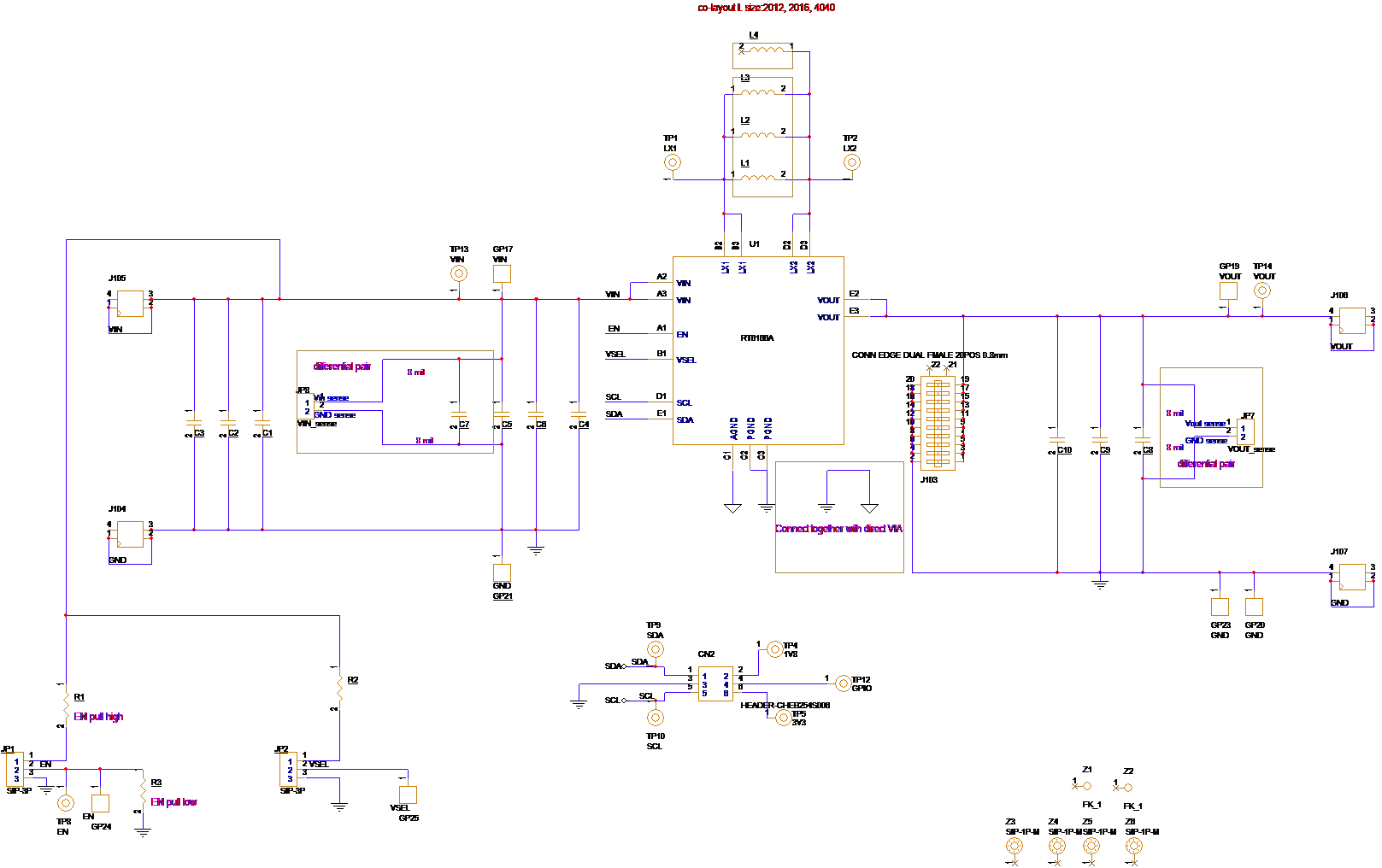
1. The capacitance values of the input and output capacitors will influence the input and output voltage ripple.
2. MLCC capacitors have degrading capacitance at DC bias voltage, and especially smaller size MLCC capacitors will have much lower capacitance.
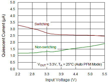
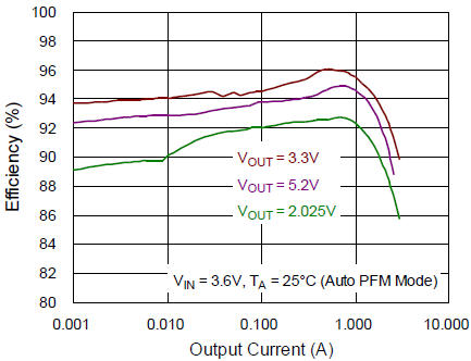
Measure Result
|
Quiescent Current vs. Input Voltage
|
Efficiency vs. Output Current
|
|
|
|
|
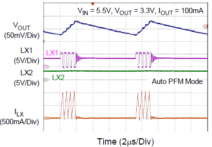
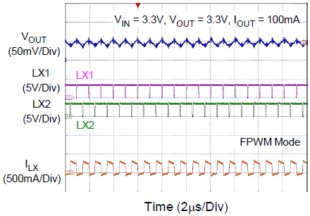
PFM Switching Waveforms
(Buck Operation)
|
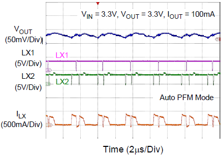
PFM Switching Waveforms
(Buck-Boost Operation)
|
|
|
|
|
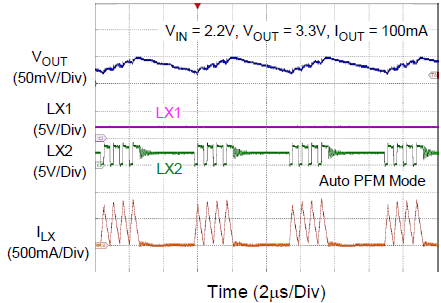
PFM Switching Waveforms
(Boost Operation)
|
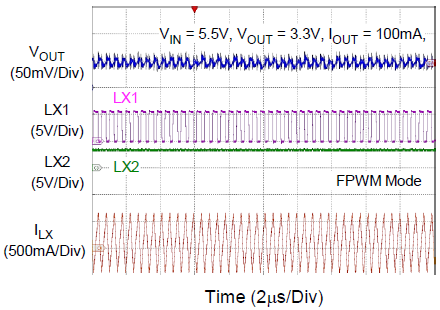
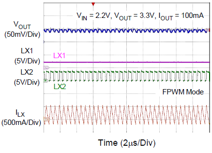
PWM Switching Waveforms
(Buck Operation)
|
|
|
|
|
PWM Switching Waveforms
(Buck-Boost Operation)
|
PWM Switching Waveforms
(Boost Operation)
|
|
|
|
|
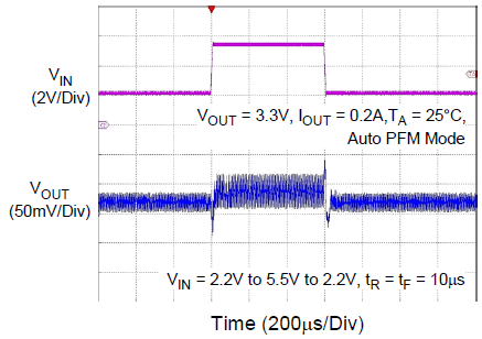
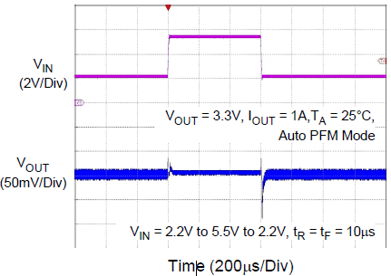
Line Transient Response (Light Load)
|
Line Transient Response (Heavy Load)
|
|
|
|
|
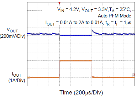
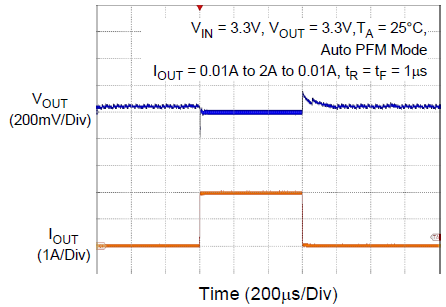
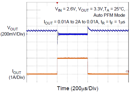
Load Transient Response (Buck)
|
Load Transient Response (Buck-Boost)
|
|
|
|
|
Load Transient Response (Boost)
|
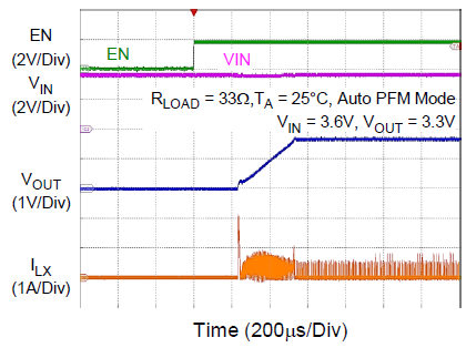
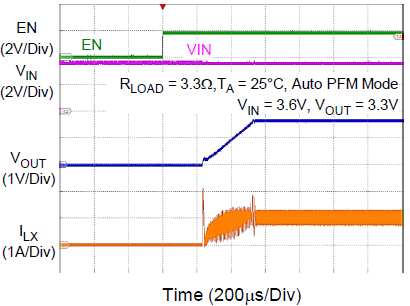
Start-Up Waveforms (Light Load)
|
|
|
|
|
Start-Up Waveforms (Heavy Load)
|
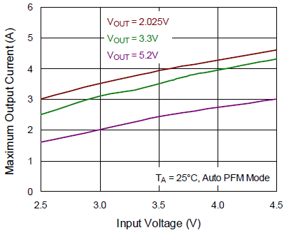
Maximum Output Current vs. Input Voltage
|
|
|
|
Note 1. When measuring the input or output voltage ripple, care must be taken to avoid a long ground lead on the oscilloscope probe. Measure the output voltage ripple by touching the probe tip directly across the output capacitor.
Evaluation Board Layout
Figure 1 to Figure 4 are RT6166DP-A’s evaluation board layout. This board size is 70mm x 50mm and is constructed on four-layer PCB.
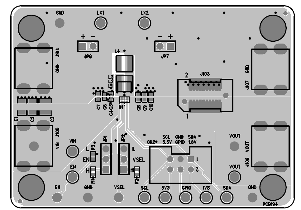
Figure 1. Top View (1st layer)
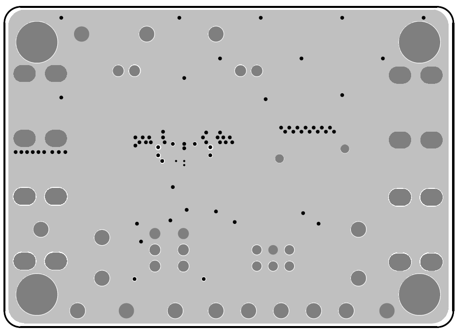
Figure 2. PCB Layout—Inner Side (2nd Layer)
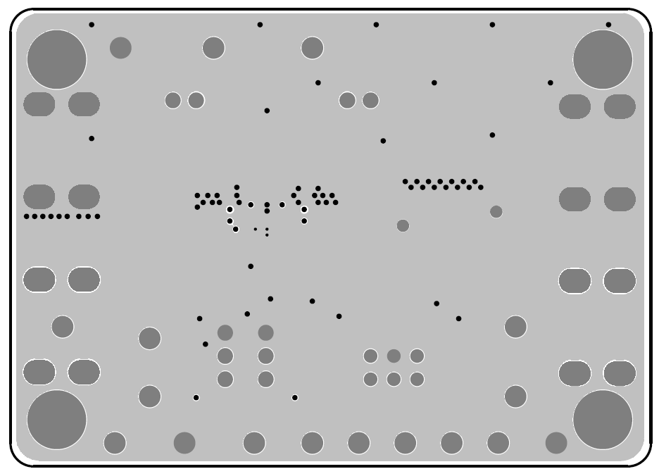
Figure 3. PCB Layout—Inner Side (3rd Layer)
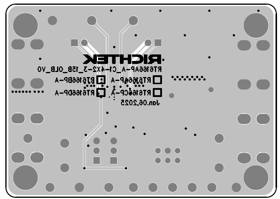
Figure 4. Bottom View (4th Layer)