Understanding Thermal Characteristic of SOT-223 Package
Abstract
For power ICs, the thermal parameters of different packages should be compliant with different applications and user’s requirements, as well as determining the thermal limits of different types of packages for the spec. Thermal parameters, such as thermal resistance θJA and θJC, are applied to determine thermal dissipation performance for integrated circuits. A low thermal resistance represents better thermal performance. A system that has a lower thermal resistance can dissipate more heat.
This article illustrates the thermal dissipation of integrated circuits with SOT-223 package, including thermal parameters and the internal structure. Finally, we will introduce the thermal analysis of PCB copper layout for SOT-223 package.
1. General Thermal Theory of Integrated Circuits
The thermal resistance is a heat property of a temperature difference by an object, which is the reciprocal of thermal conductance. In the heat flow path of specific package, there exists many heat resistance, major relating with the materials of the silicon chip, molding compound, copper of lead-frame, die attachment, and so on. In Figure 1, it is a equivalent thermal resistance model of a specific package. For which, the series of resistance is defined as Eq.(1).

Figure 1. Equivalent series of thermal resistances
θJA = θJC + θCA (1)
where,
θJC is thermal resistance from junction to case. (°C/W)
θCA is thermal resistance from case to ambient. (°C/W)
The key thermal parameter for ICs is junction temperature (TJ), which also determines stability of IC. Generally speaking, the IC datasheet will present the recommended operation temperature of junction. Since TJ cannot be measured directly, the Eq.(2) and Eq.(3) can be used for approach. In JEDEC 51 standard, the case temperature (TC) is defined at “hottest” position of the package surface and ambient temperature (TA) is defined for test environment temperature.
TJ = TA + PD x θJA (2)
TJ = TC + PD x θJC (3)
,where
θJA is thermal resistance from junction to the ambient. (°C/W)
θJC is thermal resistance from junction to the case. (°C/W)
TJ is device junction temperature in the steady state test condition. (°C)
TA is reference temperature for the ambient environment. (°C)
TC is reference temperature for the case point. (°C)
PD is power dissipation in the device. (W)
2. SOT-223 Thermal Resistance Measurement
2-1 Measurement Environment
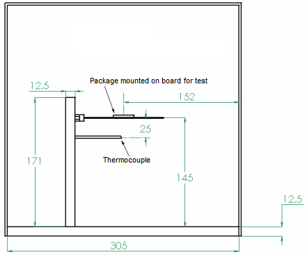
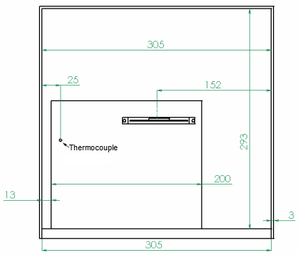
Following JEDEC 51-2 thermal measurement standard, θJA should be measured by standardized environmental condition in the natural convection (air flow = 0 ft/min) at TA = 25°C. The standardized environmental condition is presented as Figure 2 (Dimensions in mm.).
|
|
|
|
(a) Side view of the test enviromental
|
(b) End view of the test enviromental
|
|
Figure 2. Standardized environmental condition
|
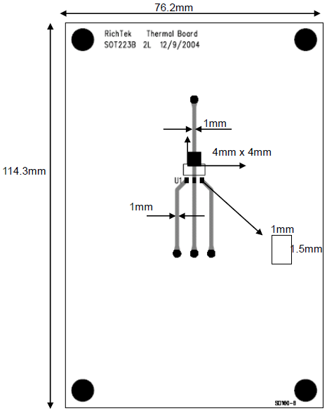
2-2 Thermal Test Board Outline
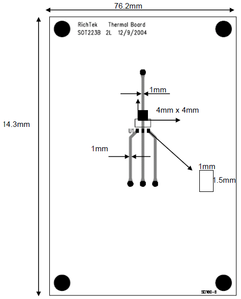
In JEDEC 51-3 and JEDEC 51-7 thermal measurement standard, the device under test is mounted on standard test boards, the detailed specifications of test board are presented as Figure 3 to Figure 6. For SOT-223 package, a 4mm x 4mm copper area and 1/mm width copper wire is designed to dissipate the thermal flow.
Low effective thermal conductivity test board layout (single layer copper, refer to JEDEC 51-3)
|
|
|
Figure 3. Single layer top view drawing
|
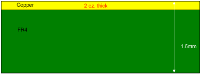
Figure 4. Single layer PCB sectional drawing
High effective thermal conductivity test board layout (Four-Layers Copper, Refer to JEDEC 51-7)
|
|
|
Figure 5. Four layers top view drawing
|
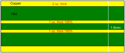
Figure 6. Four layers PCB sectional drawing
2-3 SOT-223 Thermal resistance
Base on JEDEC 51-3 and JEDEC 51-7 measurement methods, the thermal resistance of SOT-223 package, θJA and θJC, can be estimated in fixed power dissipaton and ambient temperature conditions.The mesurement result are shown as below :
l Power Dissipation, PD @ TA = 25°C, TJ = 125°C
SOT-223------------------------------------------------------------------------------------------------------------------------------- 0.741W
l Package Thermal Resistance
SOT-223, qJA------------------------------------------------------------------------------------------------------------------------ 135°C/W
SOT-223, qJC------------------------------------------------------------------------------------------------------------------------ 15°C/W
3. Thermal Characteristics of SOT-223 Package Structure
3-1 SOT-223 Package Structure Material Characteristics
Base on Eq.(2), the lower resistance means that the junction temperature will be lower in the same power dissipation and ambient temperature, and the thermal conductivity of package material will dominate the thermal resistance of package. Therefore, the SOT-223 package utilizes high thermal conductance of lead frame to decrease the thermal resistance. The SOT-223 package internal structure is shown in Figure 7, and the physical dimension parameters and material properties of the components used in this model are summarized in Table 1.
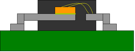
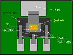
Figure 7. SOT-223 Top and section transparent view drawing
Table 1. Physical dimension parameters and material properties
|
COMPONET DIMENSION
|
|
Compound Size (mm)
|
3.5 x 6.5 x 1.8
|
|
Die Size (mm)
|
0.700 x 0.700
|
|
Die Thickness (mil)
|
12
|
|
Die Attach Thickness (mil)
|
0.4
|
|
Pad Size (mm)
|
2.50 x 3.00
|
|
Leadframe Thickness (mm)
|
0.305
|
|
PCB Thickness (oz.)
|
2
|
|
THERMAL CONDUCTIVITY (W/m°C)
|
|
Compound
|
0.847
|
|
Die
|
140
|
|
Die Attach
|
2.5
|
|
Pad & Leadframe
|
284
|
|
FR-4
|
0.3
|
|
Copper
|
385
|
|
Solder
|
51
|
In Figure 8, it is very specificaly difference of structure between SOT-223 and other packages. In SOT-223 package, the die, thermal soure, is directly connected to exposed lead frame, and the major thermal flow can be conducted through the exposed lead frame to PCB trace and ambient. However, other packages only use gold wires to connect the die and the lead frame. That makes thermal resistance of SOT-223 smaller than other packages. As a result, we can use this characteristic to improve the thermal performance by designing the PCB copper layout on SOT-223 package.
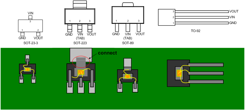
Figure 8. SOT-223 packages transparent view drawing
3-2 Thermal Performance Enhancerment of SOT-223 Package
Beacuse of the structure of SOT-223 package, the thermal resistance can be improved by adding copper area under the exposed lead frame. Figure 9 shows the relationship between the copper area and the thermal resistance θJA. When IC is mounted to the standard footprint (16mm2), the thermal resistance θJA is 135°C/W, adding copper area of pad to 100mm2 under the package reduces the θJA to 107°C/W. Even further, increasing the copper area of pad to 2500mm2 reduces the θJA to 50°C/W.
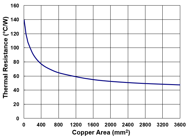
Figure 9. SOT-223 thermal resistance θJA. vs. PCB copper area
As shown in Figure 9, we can also find the SOT-223 maximum power dissipation improvement by different copper area design at ambient temperature TA = 25°C operation.
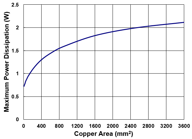
Figure 10. Maximum power dissipation PD. vs. PCB copper area
For the SOT-223 packages, the de-rating curves in Figure 11 allow the designer to see the effect of rising ambient temperature on the maximum power dissipation.
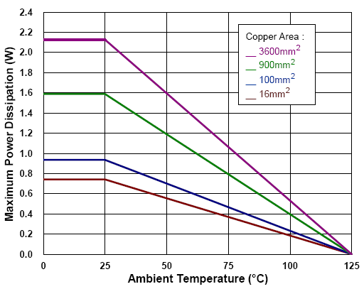
Figure 11. De-rating curves for SOT-223 packages
4. Conclusions
According to the above discussion of thermal resistance and junction temperature, it was found that the thermal resistance affects dissipative heat of the system. We must follow the maximum power dissipation (power limit) and maximum junction to ambient thermal resistance requirements. If the selected package can’t satisfy the requirement of thermal resistance restrictions, PCB layout needs to be improved to keep IC junction temperature below 125°C. Hence, for high power IC series products with a variety of power dissipations, adding proper copper area is essential.
This article provides a general thermal concept for SOT-223 package. Many estimations and generalizations have been used. Please refer to these information as a generally approximation of required board copper area. If customers need further thermal information on any system level design, please contact us.