Purpose
The RT2862 is a high-efficiency current mode synchronous step-down regulator that can deliver up to 3A output current from a wide input voltage range of 4.5V to 36V. This document explains the function and use of the RT2862 evaluation board (EVB) and provides information to enable operation and modification of the evaluation board and circuit to suit individual requirements.
Introduction
General Product Description
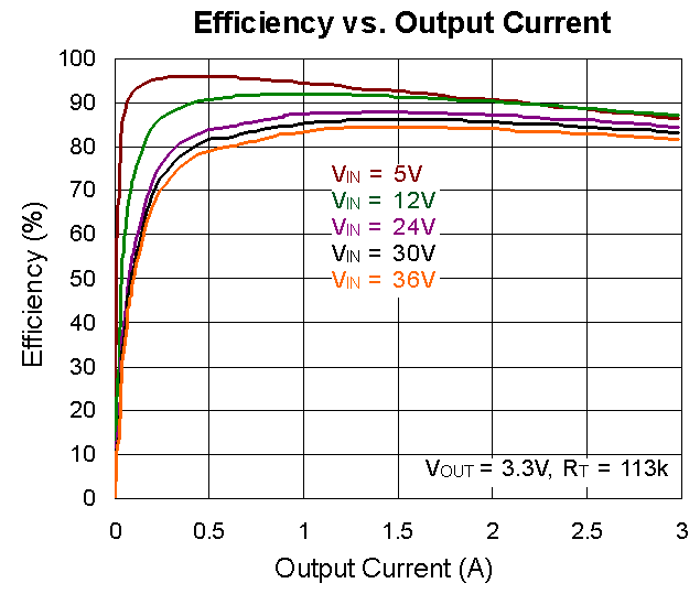
The RT2862 is a high efficiency, current mode synchronous step-down DC/DC converter that can deliver up to 3A output current over a wide input voltage range from 4.5V to 36V. The device integrates a 105mΩ high side and an 80mΩ low side MOSFET to achieve high conversion efficiency up to 95%. The current mode control architecture supports fast transient response and uses a simple compensation circuit.
A cycle-by-cycle current limit function provides protection against a shorted output and an internal soft-start eliminates input surge current during start-up. The RT2862 provides complete protection functions such as input under voltage lockout, output under voltage protection, over current protection and thermal shutdown.
The RT2862 is available in the thermal enhanced SOP-8 (Exposed Pad) package.
Product Features
- 4.5V to 36V Input Voltage Range
- 3A Output Current
- Internal N-MOSFETs
- Current Mode Control
- Frequency Operation : 300kHz to 1MHz
- Adjustable Output Voltage from 0.8V to 30V
- High Efficiency Up to 95%
- Stable with Low ESR Ceramic Output Capacitors
- Cycle-by-Cycle Current Limit
Application
- Point of Load Regulator in Distributed Power Systems
- Digital Set Top Boxes
- Broadband Communications
- Vehicle Electronics
- Automotive Audio, Navigation, and Information Systems
- Enterprise Datacom Platforms Point of Load (POL)
- Industrial Grade General Purpose Point of Load
Evaluation Board
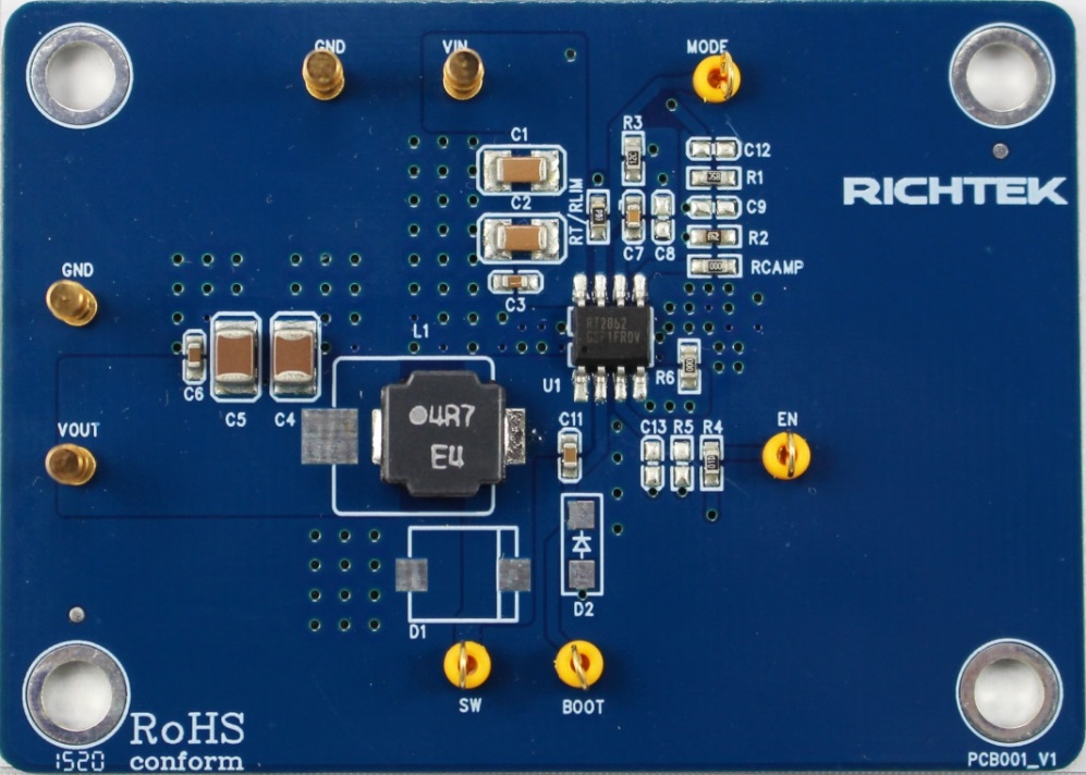
Please carefully inspect the EVB IC and external components, comparing them to the following Bill of Materials, to ensure that all components are installed and undamaged. If any components are missing or damaged during transportation, please contact the distributor or send e-mail to evb_service@richtek.com
Test Points
The EVB is provided with the test points and pin names listed in the table below.
|
Test point/Pin name
|
Signal
|
Comment (expected waveforms or voltage levels on test points)
|
|
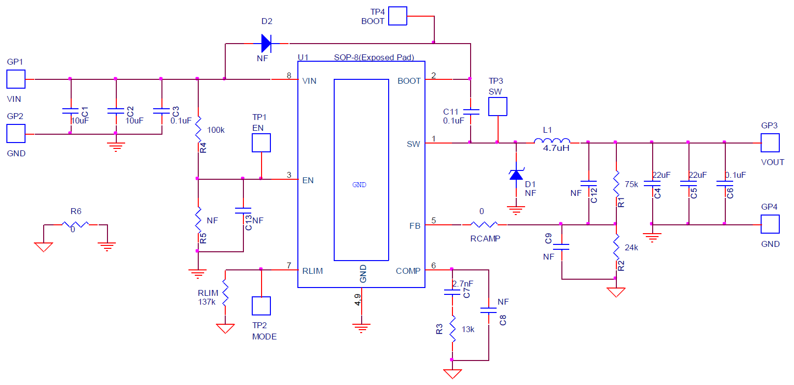
VIN
|
Input voltage
|
Input voltage range = 4.5V to 36V
|
|
VOUT
|
Output voltage
|
Default output voltage = 3.3V
Output voltage range = 0.8V to 30V
(see ‘’ Output Voltage Setting’’ section for changing output voltage level)
|
|
SW
|
Switch Node
|
SW waveform
|
|
EN
|
Chip Enable Operation
|
Enable signal. EN is automatically pulled high (by R4) to enable operation. Connect EN low to disable operation.
|
|
BOOT
|
Boot strap supply test point
|
Floating supply voltage for the high-side N-MOSFET switch
|
|
MODE
|
RT test point
|
Switching frequency setting point
|
|
GND
|
Ground
|
Ground
|
Power-up & Measurement Procedure
1. Apply a 12V nominal input power supply (4.5V < VIN < 36V) to the VIN and GND terminals.
2. The EN voltage is pulled to logic high by R4 (100kΩ to VIN) to enable operation. Drive EN high (>2.0V) to enable operation or low (<0.4V) to disable operation.
3. Verify the output voltage (approximately 3.3V) between VOUT and GND.
4. Connect an external load up to 3A to the VOUT and GND terminals and verify the output voltage and current.
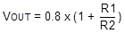
Output Voltage Setting
Set the output voltage with the resistive divider (R1, R2) between VOUT and GND with the midpoint connected to FB through RCAMP. The output is set by the following formula:
The installed VOUT capacitors (C4, C5) are 22μF, 16V X5R ceramic types. Do not exceed their operating voltage range and consider their voltage coefficient (capacitance vs. bias voltage) and ensure that the capacitance is sufficient to maintain stability and provide sufficient transient response for your application. This can be verified by checking the output transient response as described in the RT2862 IC datasheet.
Specification
|
Parameter
|
Symbol
|
Min
|
Typ.
|
Max
|
Units
|
|
Input Voltage Range
|
VIN
|
4.5
|
|
36
|
V
|
|
Output Voltage
|
VOUT
|
|
3.3
|
|
V
|
|
Oscillator Frequency
|
fOSC
|
300k
|
|
1M
|
Hz
|
|
Output Current
|
IOUT
|
|
|
3
|
A
|
|
High-Side Switch Current Limit
Range
|
UOC
|
4.25
|
5
|
5.75
|
A
|
Schematic
BOM
|
Reference
|
Q'ty
|
P/N
|
Description
|
Package
|
Manufacture
|
|
U1
|
1
|
RT2862GSP
|
DC/DC Converter
|
PSOP-8
|
Richtek
|
|
C1, C2
|
2
|
C3216X5R1H106K160AB
|
10μF/±10%/50V/X5R
Ceramic Capacitor
|
1206
|
TDK
|
|
C4, C5
|
2
|
GRM32ER61C226KE20#
|
22μF/±10%/16V/X5R
Ceramic Capacitor
|
1210
|
Murata
|
|
C7
|
1
|
0603B272K500
|
2.7nF/±10%/50V/X7R
Ceramic Capacitor
|
0603
|
WALSIN
|
|
C3, C6, C11
|
3
|
C1608X7R1H104K080AA
|
0.1μF/±10%/50V/X7R
Ceramic Capacitor
|
0603
|
TDK
|
|
C8, C9, C12, C13
|
0
|
|
Not Installed
|
0603
|
|
|
L1
|
1
|
NR8040T4R7N
|
4.7μH/4.1A
|
8 x 8 x 4.2mm
|
TAIYO YUDEN
|
|
R1
|
1
|
|
75kΩ/±1%, Resistor
|
0603
|
|
|
R2
|
1
|
|
24kΩ/±1%, Resistor
|
0603
|
|
|
R3
|
1
|
|
13kΩ/±1%, Resistor
|
0603
|
|
|
R4
|
1
|
|
100kΩ/±1%, Resistor
|
0603
|
|
|
R5, D1, D2
|
0
|
|
Not Installed
|
|
|
|
R6, RCAMP
|
2
|
|
0Ω, Resistor
|
0603
|
|
|
RT
|
1
|
|
113kΩ/±1%, Resistor
|
0603
|
|
|
TP
|
4
|
|
Test Pin
|
|
|
|
GP
|
4
|
|
Golden Pin
|
|
|
PCB Layout
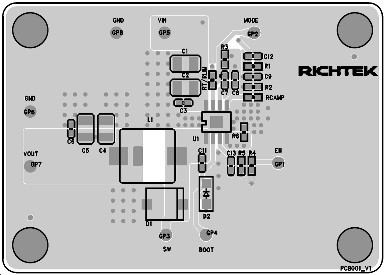
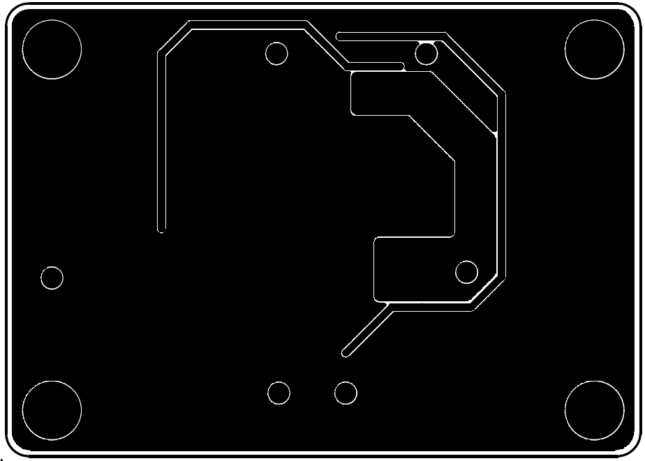
Top View (1st layer)
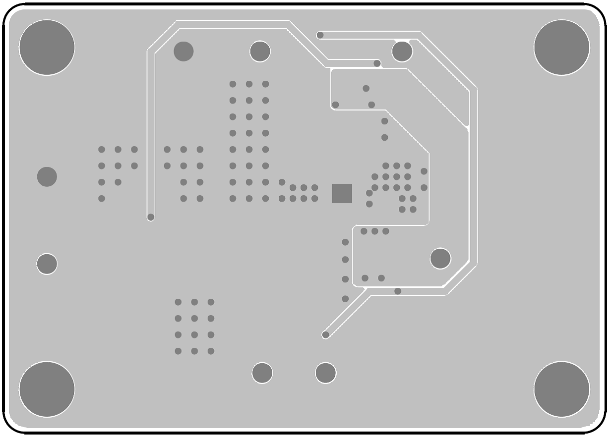
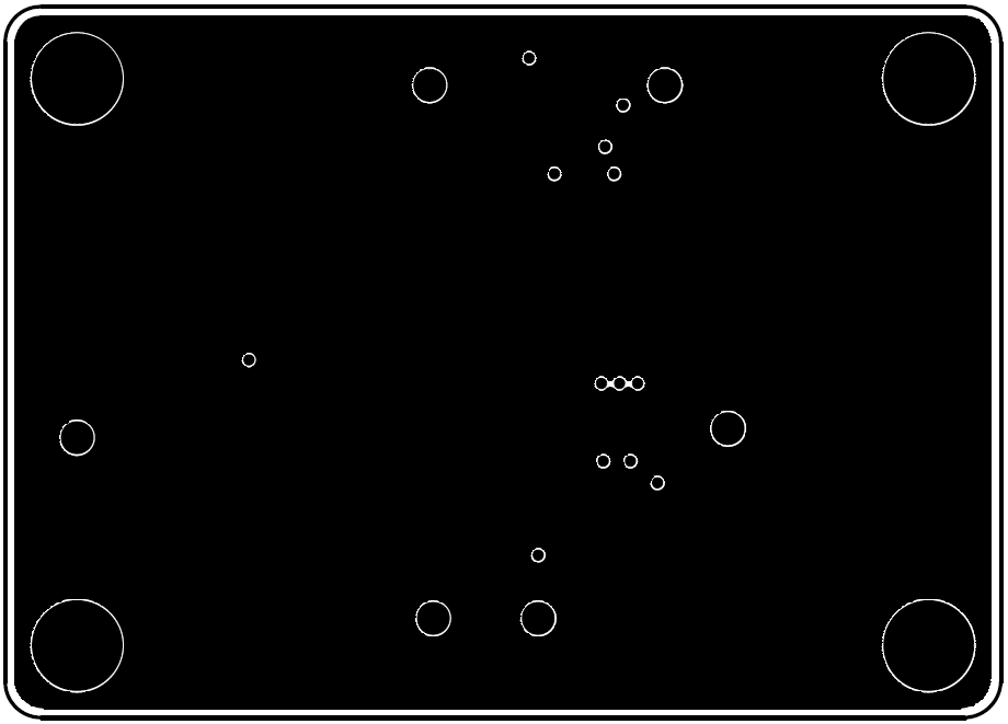
Bottom View (4th Layer)
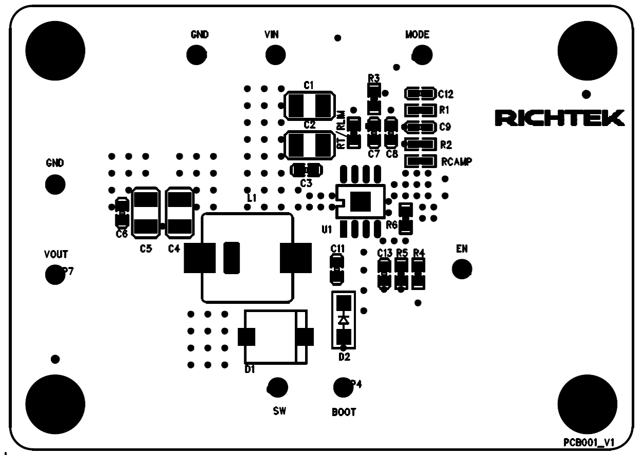
Component Placement Guide—Component Side (1st layer)
PCB Layout—Component Side (1st Layer)
PCB Layout—Inner Side (2nd Layer)
PCB Layout—Inner Side (3rd Layer)
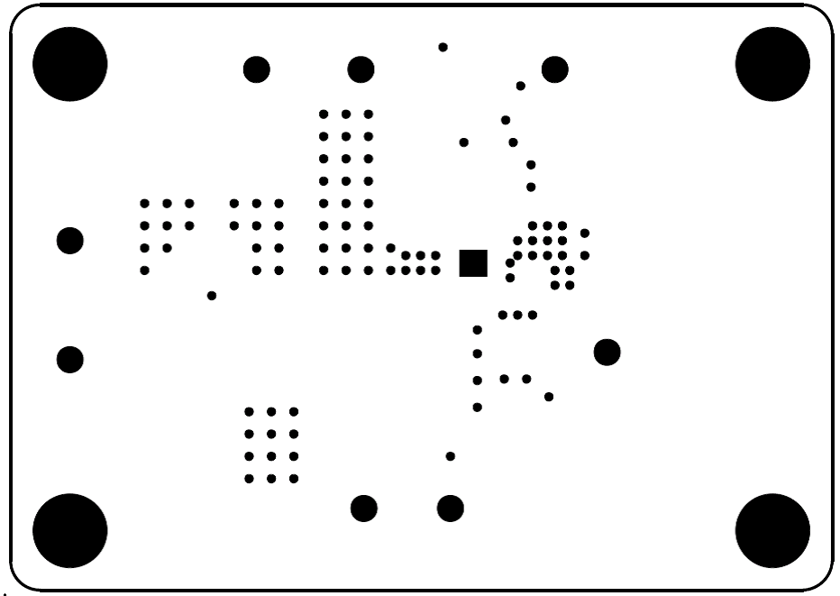
Component Placement Guide—Bottom Side (4th Layer)
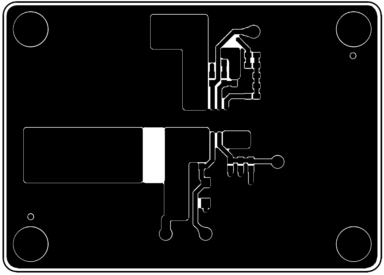
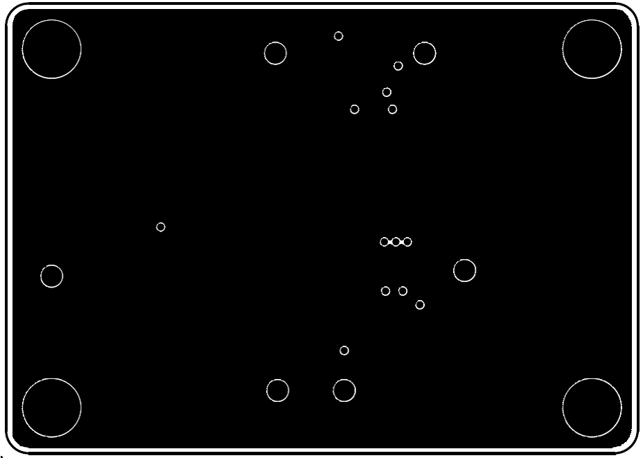
PCB Layout—Bottom Side (4th layer)
Step-Down Converter Efficiency Test