Purpose
The RT5797A is a high efficiency synchronous step-down DC-DC converter. Its input voltage range is from 2.7V to 6V and provides an adjustable regulated output voltage from 0.6V to 3.4V while delivering up to 3A of output current. This document explains the function and use of the RT5797A evaluation board (EVB), and provides information to enable operation, modification of the evaluation board and circuit to suit individual requirements.
Introduction
General Product Information
The RT5797A is a high efficiency synchronous step-down DC-DC converter. Its input voltage range is from 2.7V to 6V and provides an adjustable regulated output voltage from 0.6V to 3.4V while delivering up to 3A of output current. The internal synchronous low on-resistance power switches increase efficiency and eliminate the need for an external Schottky diode. The RT5797A is available in the WDFN-8SL 2x2 packages.
Product Feature
- Efficiency Up to 95%
- RDS(ON) 100mΩ HS / 70mΩ LS
- VIN Range 2.7V to 6V
- VREF 0.6V with ±1% Accuracy at 25℃
- CMCOTTM Control Loop Design for Best Transient Response, Robust Loop Stability with Low-ESR (MLCC) COUT
- Fixed Soft-Start 1.2ms
- Power Saving in Light Load
Key Performance Summary Table
|
Key Features
|
Evaluation Board Number : PCB103_V1
|
|
Default Input Voltage
|
5V
|
|
Max Output Current
|
3A
|
|
Default Output Voltage
|
1.2V
|
|
Default Marking & Package Type
|
RT5797AHGQWA, WDFN-8SL 2x2
|
|
Operation Frequency
|
1MHz in CCM mode
|
Bench Test Setup Conditions
Headers Description and Placement
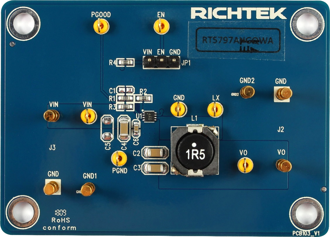
Carefully inspect all the components used in the EVB according to the following Bill of Materials table, and then make sure all the components are undamaged and correctly installed. If there is any missing or damaged component, which may occur during transportation, please contact our distributors or e-mail us at evb_service@richtek.com.
Test Points
The EVB is provided with the test points and pin names listed in the table below.
|
Test point/
Pin name
|
Signal
|
Comment (expected waveforms or voltage levels on test points)
|
|
FB
|
Feedback Voltage Input
|
An external resistor divider from the output to SGND, tapped to the FB pin, sets the output voltage. keep away from high current loops and swithing voltages.
|
|
PGOOD
|
Power Good Indicator
|
The output of this pin is an open-drain with external pull-up resistor. PG is pulled up when the FB voltage is within 90%, otherwise it is LOW.
|
|
VIN
|
Supply Voltage Input
|
The RT5797A operates from a 2.7V to 6V input.
|
|
PGND, GND GND1, GND2
|
Power Ground
|
Power ground. The exposed pad must be soldered to a large PCB and connected to PGND for maximum thermal dissipation.
|
|
NC
|
No Internal Connection
|
No internal connection.
|
|
LX
|
Switch Node
|
Switch node.
|
|
EN
|
Enable Control Input
|
Enable control input. A logic-high enables the converter; a logic-low forces the device into shutdown mode.
|
|
SGND
|
Signal Ground
|
Signal ground of the FB network. SGND should be connected to PGND close to the IC PGND pins.
|
|
VO
|
Output voltage
|
Output voltage.
|
Power-up & Measurement Procedure
1. Apply a 5V nominal input power supply (2.7V < VIN < 6V) to the VIN and GND terminals.
2. Set the jumper at JP1 to connect terminals 2 and 3, connecting EN to VIN through resistor R4 (100kΩ). The Enable pin can connected to VIN directly as well to enable operation.
3. Verify the output voltage (approximately 1.2V) between VOUT and GND.
4. Connect an external load up to 3A to the VOUT and GND terminals and verify the output voltage and current.
Output Voltage Setting
Set the output voltage with the resistive divider (R1, R2) between VOUT and GND with the midpoint connected to FB. The output is set by the following formula :

The placement of the resistive divider should be within 5mm of the FB pin. The resistance of R2 is suggested between 10kΩ and 150kΩ to minimize power consumption, and noise pick-up at the FB pin. The resistance of R1 can then be obtained as below :

For better output voltage accuracy, divider resistors (R1 and R2) should have tolerance of ±1% tolerance or better.
Schematic, Bill of Materials & Board Layout
EVB Schematic Diagram
RT5797AHGQW demo board : VIN 5V, VOUT 1.2V / 3A

Note:
1. Do not hot-plug a live 5V supply to the board; if hot-plugging is required, add ~100µF electrolytic capacitor at the input.
A small feedforward capacitor (C1) can be introduced into the feedback network to speed up the transient response of high output voltage circuits. Adding C1 can also improve the light load PSM switching behavior. The feedforward capacitor is added across the upper FB divider.
To optimize transient response, C1 value is chosen so that the gain and phase boost of the feedback network increases the bandwidth of the converter, while still maintaining an acceptable phase margin. Generally, larger C1 values provide higher bandwidth, but may result in an unacceptable phase margin or instability.
Measurement Results
|
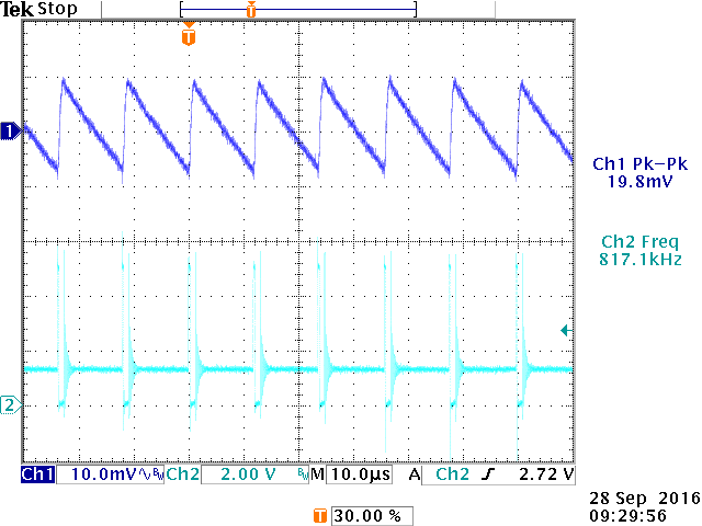
Output ripple measurement at VIN = 5V 10mA load
Cyan : V-SW; Blue : VOUT
|
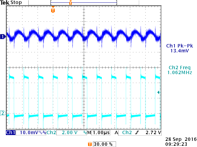
Output ripple measurement at VIN = 5V 3A load
Cyan : V-SW; Blue : VOUT
|
|
|
|
|
Output ripple at 10mA load : 19.8mVpp, PSM mode
|
Output ripple at 3A load : 13.4mVpp
PWM frequency is 1.062kHz.
|
|
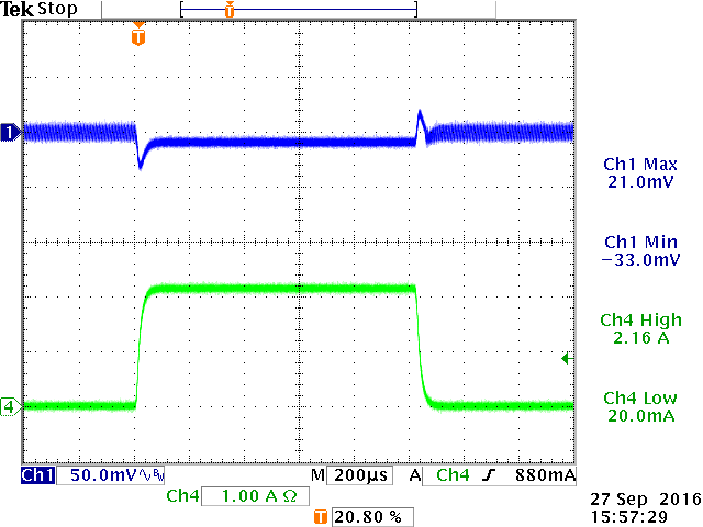
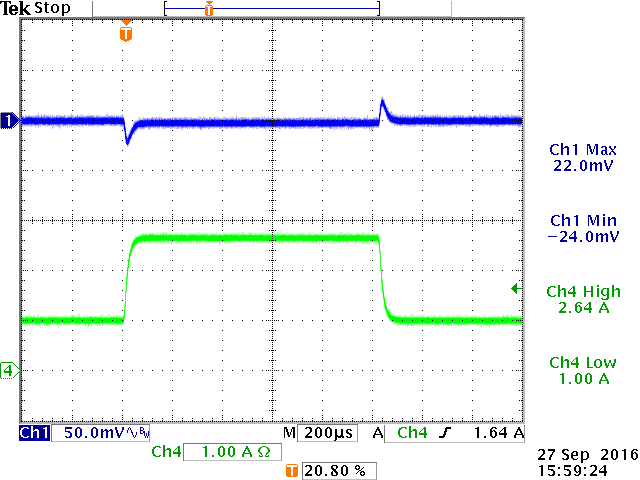
Dynamic load 0.01A to 2.2A load step
Blue : VOUT; Green : load current step
|
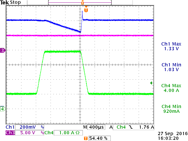
Dynamic load 1A to 2.6A load step
Blue : VOUT; Green : load current step
|
|
|
|
|
Overshoot : 21mV, Undershoot : 33mV in light load mode
|
Overshoot : 22mV, Undershoot : 24mV
|
|
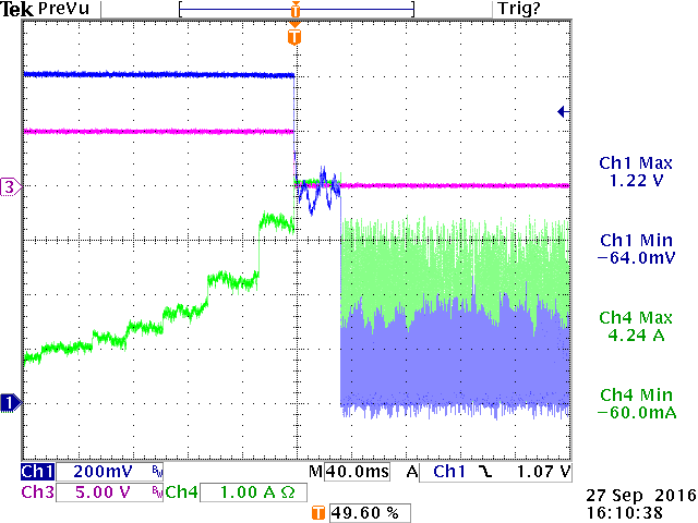
OCP measurement : Dynamic load close to OCP
Blue: VOUT; Purple: Pgood; Green: Iout
|
OCP measurement : Full output short circuit
Blue: VOUT; Purple: Pgood; Green: Iout
|
|
|
|
|
Vout drops at 4A peak load.
|
Frequency reduction, hiccup mode at 4.24A peak load current
|
|
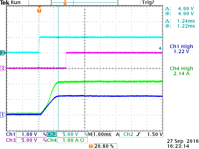
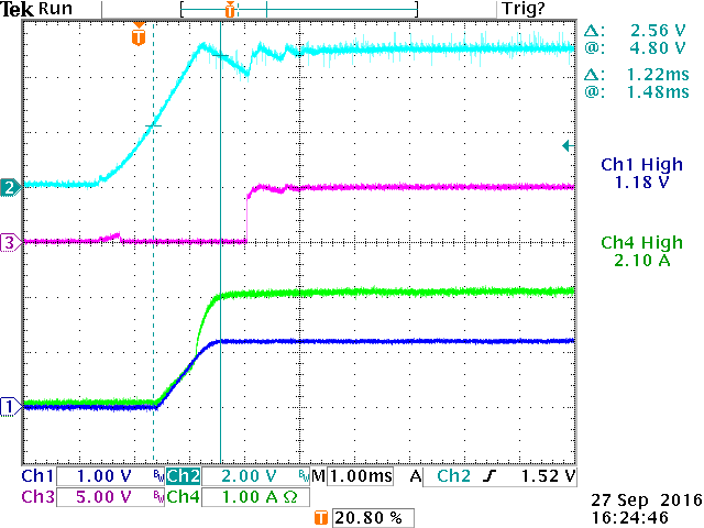
Start-up measurement from Enable :
EN pin 7 low – high
Cyan : V-Enable; Blue:VOUT; Purple : Pgood; Green : IOUT
|
Start-up measurement from VIN :
Cyan : VIN; Blue : VOUT; Purple : Pgood; Green : IOUT
|
|
|
|
|
Start-up time 1.24msec. Soft-start 1.1msec
|
VIN > 2.24V initiates start-up.
|
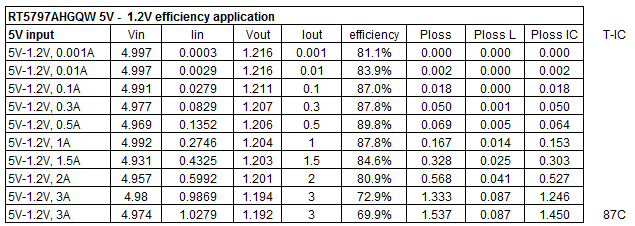
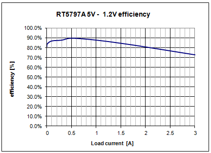
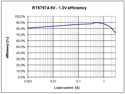
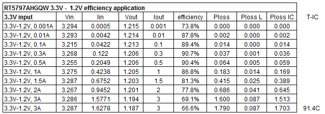
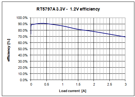
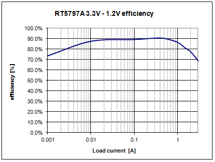
Efficiency Measurements
Bill of Materials
|
Reference
|
Qty
|
Part Number
|
Description
|
Package
|
Manufacturer
|
|
U1
|
1
|
RT5797AHGQWA
|
DC-DC Converter
|
WDFN-8SL 2x2
|
Richtek
|
|
C1
|
1
|
|
NC
|
C-0603
|
|
|
C2, C3, C4
|
3
|
GRM31CR61C226KE15L
|
22µF/16V/X5R/1206
|
C-1206
|
muRata
|
|
C5
|
1
|
|
NC
|
C-1206
|
|
|
C6
|
1
|
GRM188R71H104KA93D
|
100nF/50V/X7R/0603
|
C-0603
|
muRata
|
|
L1
|
1
|
7447714015
|
1.5µH
|
10x10x5mm
|
WURTH ELEKTRONIK
|
|
R1, R2, R3, R4
|
4
|
WR06X1003FTL
|
100k/0603
|
R-0603
|
WALSIN
|
PCB Layout
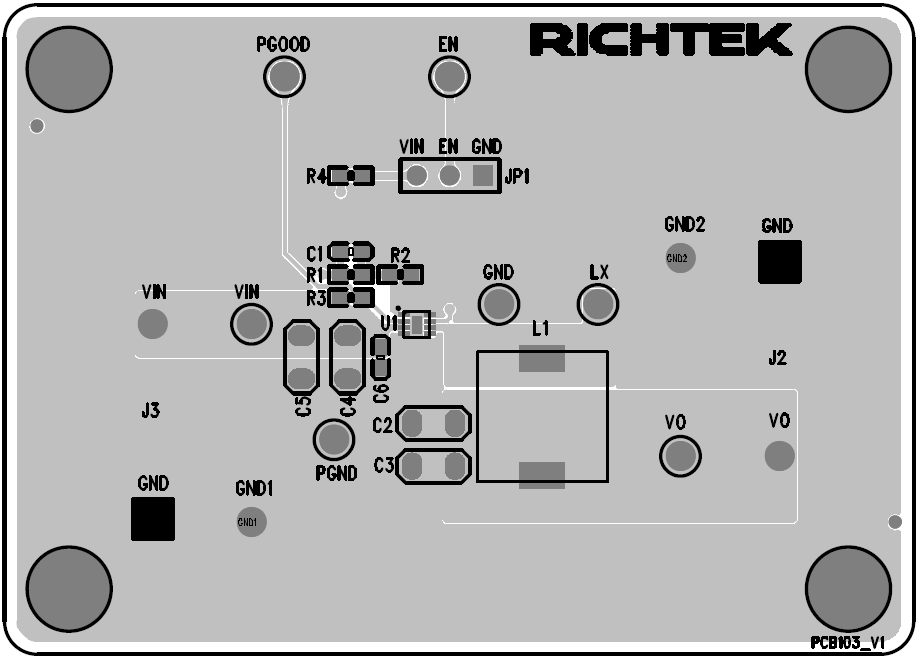
Top View (1st layer)

PCB Layout—Inner Side (2nd Layer)

PCB Layout—Inner Side (3rd Layer)
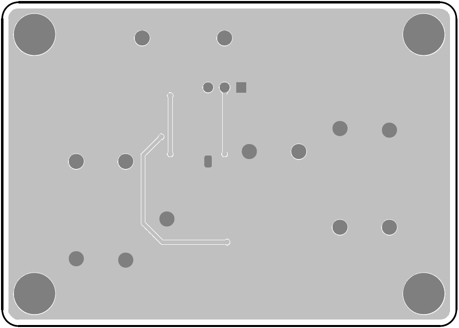
Bottom View (4th Layer)