Purpose
The RT9118 is a Audio Amplifier the input voltage range from 8V to 17V. This document explains the function and use of the RT9118 evaluation board (EVB), and provides information to enable operation, modification of the evaluation board and circuit to suit individual requirements.
Introduction
General Product Information
The RT9118 is a 10W per channel, high efficiency Class D stereo audio amplifier for driving bridge tied load (BTL) speakers. The RT9118 can drive stereo speakers with load as low as 4Ω. Its high efficiency eliminates the need for an extra heat sink when playing music. The gain of the amplifier can be controlled by gain select pins. The outputs are fully protected against shorts to GND, PVCC, and output to output with an auto recovery feature and monitored output.
Product Feature
- 8V to 17V Input Supply Range
►10W / CH for an 8Ω Load, 13V Supply at 10% THD + N
►15W / CH for an 8Ω Load, 16V Supply at 10% THD + N
►90% Efficiency Eliminates Need for Heat Sinks
- Two Selectable Gain Settings
- Over-Temperature Protection (OTP) with Auto Recovery Option
- Surface Mount 28-Lead WQFN Package
Key Performance Summary Table
|
Key Features
|
Evaluation Board Number : PCB086_V1
|
|
PVCC Input Voltage
|
12V
|
|
HPVDD Input Voltage
|
5V
|
|
Speaker Output Power (Load=8Ω, THD+N=10%)
|
9W
|
|
Headphone Output Power (Load=16Ω, THD+N=1%)
|
30mW
|
|
Marking & Package Type
|
RT9118GQW, WQFN-28L 4x5
|
Bench Test Setup Conditions
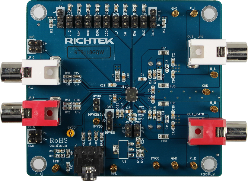
Headers Description and Placement
Carefully inspect all the components used in the EVB according to the following Bill of Materials table, and then make sure all the components are undamaged and correctly installed. If there is any missing or damaged component, which may occur during transportation, please contact our distributors or e-mail us at evb_service@richtek.com.
Test Points
The EVB is provided with the test points and pin names listed in the table below.
|
Test point/
Pin name
|
Signal
|
Comment (expected waveforms or voltage levels on test points)
|
|
PVCC
|
Input power supply
|
Power input. Support 8V to 17V Input Voltage.
|
|
EN
|
Enable test point
|
High = Enable, Low = Disable.
|
|
GND
|
Ground
|
Ground.
|
|
Audio IN
|
Analog source input
|
Stereo analog source input.
|
|
SPK OUT
|
Speaker Output
|
Stereo analog to Speaker Amplifier. (Left & Right Channel Output)
|
|
HP OUT
|
Headphone Output
|
Stereo analog to Headphone Amplifier. (Headphone Output)
|
|
Gain
|
Gain setting
|
Gain test-pin, High = 31dB, Low = 26dB.
|
|
Plimit
|
Plimit setting
|
Power Limit Level. (5W, 10W, MAX) (Short = Enable, Open = Disable)
|
Power-up & Measurement Procedure
1. Connect input power supply (8V < PVCC < 17V) and ground to PVCC and GND pins respectively.
2. Connect input power supply (HPVDD = 5V) and ground to HPVDD and GND pins respectively.
3. The 1X3 Header (GAIN) is the Gain setting. (High = 32dB, Low = 26dB).
4. The 1X2 Header (5W, 10W, MAX) is the Plimit setting. (Short = Enable, Open = Disable).
5. The 1X3 Header (JD) is the JD setting. (High = HP mode, Low = SPK mode).
6. Connect stereo analog source input to IN_L (L_CH Input), IN_R (R_CH Input) RCA Jack.
7. Connect speaker to the GP1 (P_L), GP2 (N_L), GP3 (P_R), GP4 (N_R).
8. Connect headphone to the GP5 (HPL), GP8 (HPR).
9. The 1X3 Header (EN) is the Enable controlled. (High = Enable, Low = Disable).
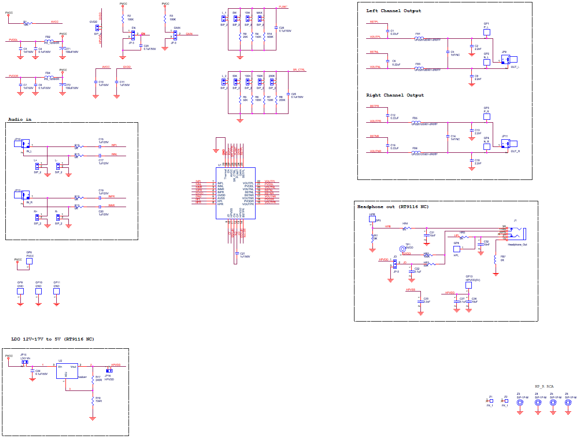
Schematic, Bill of Materials & Board Layout
EVB Schematic Diagram
Bill of Materials
|
Reference
|
Qty
|
Part number
|
Description
|
Package
|
Manufacturer
|
|
U1
|
1
|
RT9118GQW
|
10W stereo Class-D Speaker Amplifier
|
WQFN-28L 4x5
|
Richtek
|
|
CT1, CT2
|
2
|
CT100F
|
100μF/50V
|
EC-2P_8
|
JACKCON
|
|
C1, C6, C12, C16
|
4
|
C1608X5R1C224K
|
0.22μF/16V/X5R
|
C-0603
|
TDK
|
|
C2, C9, C13, C18
|
4
|
C1608X5R1H222K
|
2.2nF/50V/X5R
|
C-0603
|
TDK
|
|
C3, C7
|
2
|
C1608X5R1H102K
|
1nF/50V/X5R
|
C-0603
|
TDK
|
|
C4, C8, C25, C28, C29
|
5
|
C1608X5R1H104K
|
0.1μF/50V/X5R
|
C-0603
|
TDK
|
|
C10, C11, C21
|
3
|
C1608X5R1H105K
|
1μF/50V/X5R
|
C-0603
|
TDK
|
|
C15, C17, C19, C20
|
4
|
C1608X5R1E105K
|
1μF/25V/X5R
|
C-0603
|
TDK
|
|
C22, C27
|
2
|
C1608X5R1E104K
|
0.1μF/25V/X5R
|
C-0603
|
TDK
|
|
C23
|
1
|
C2012X5R1C225K
|
2.2μF/16V/X5R
|
C-0805
|
TDK
|
|
C26
|
1
|
C2012X5R1C106K
|
10μF/16V/X5R
|
C-0805
|
TDK
|
|
C31, C32
|
2
|
C1608X5R1H103K
|
10nF/50V/X5R
|
C-0603
|
TDK
|
|
FB1, FB3, FB5, FB6
|
4
|
UPZ2012E601-2R0TF
|
600Ω±25%
|
0805
|
Sunlord
|
|
FB2, FB4
|
2
|
RTT05000JTP
|
0R/0805/±5%
|
R-0805
|
Ralec
|
|
FB7, R10, R11, R12, R13
|
5
|
WR06X000PTL
|
0R/0603/±1%
|
R-0603
|
WALSIN
|
|
J1
|
1
|
Headphone Jack
|
Headphone_Out
|
LJE0364-5
|
Lih Sheng
|
|
R1
|
1
|
WR08X10R0FTL
|
10R/0805/±1%
|
R-0805
|
WALSIN
|
|
R2, HR2, R3, R6
|
4
|
WR06X1003FTL
|
100K/0603/±1%
|
R-0603
|
WALSIN
|
|
R4, R7
|
2
|
WR06X1503FTL
|
150K/0603/±1%
|
R-0603
|
WALSIN
|
|
R8
|
1
|
WR06X2003FTL
|
200K/0603/±1%
|
R-0603
|
WALSIN
|
|
R9
|
1
|
WR06X2492FTL
|
24.9K/0603/±1%
|
R-0603
|
WALSIN
|
|
R14
|
1
|
WR06X4993FTL
|
499K/0603/±1%
|
R-0603
|
WALSIN
|
|
HR1
|
1
|
WR06X1002FTL
|
10K/0603/±1%
|
R-0603
|
WALSIN
|
|
HR3, R5
|
2
|
RTT034992FTP
|
49.9K/0603/±1%
|
R-0603
|
Ralec
|
|
HR4, HR5
|
2
|
WR06W2R20FTL
|
2.2R/0603/±1%
|
R-0603
|
WALSIN
|
PCB Layout
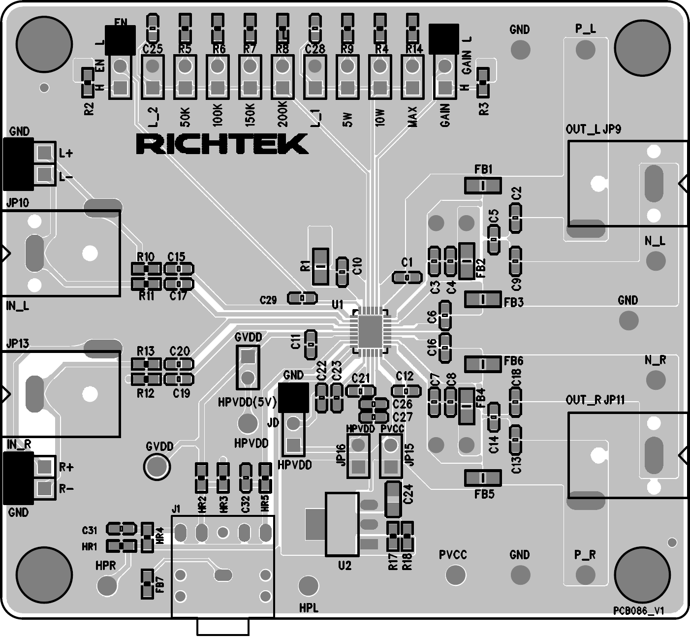
Top View (1st layer)

PCB Layout—Inner Side (2nd Layer)

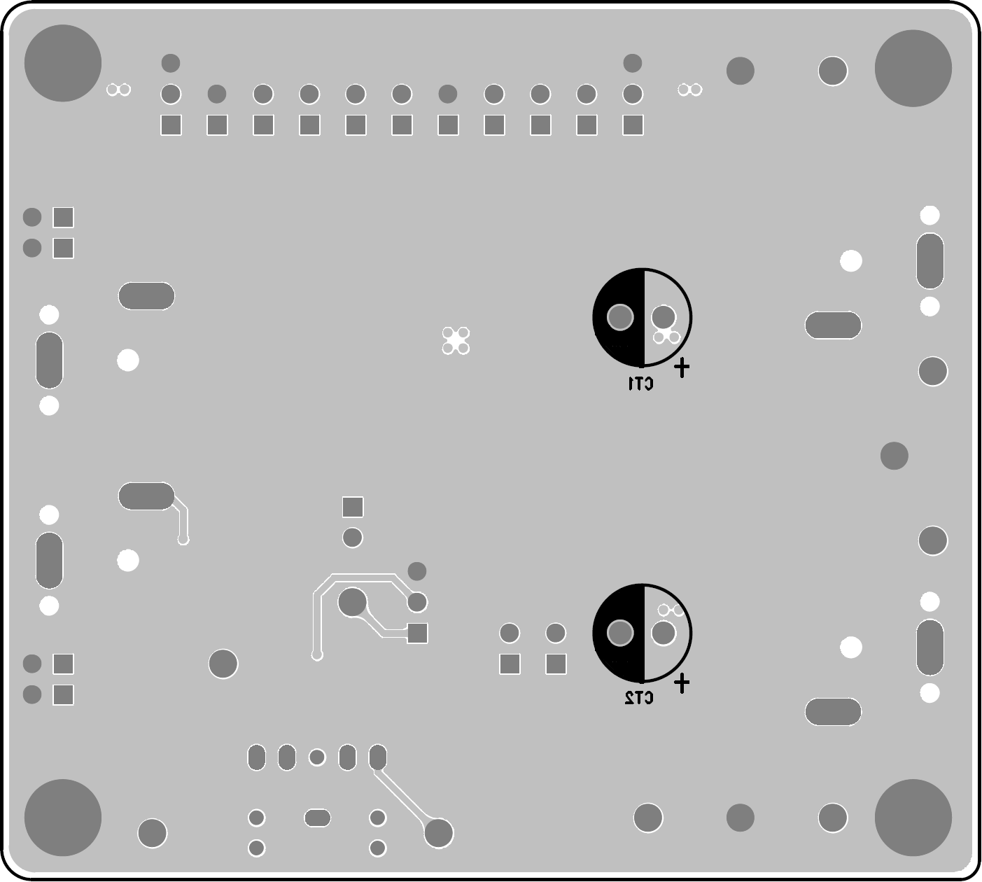
PCB Layout—Inner Side (3rd Layer)
Bottom View (4th Layer)