Purpose
The RT9742A is a cost-effective, low-voltage, single N-MOSFET high-side Power Switch IC for USB application. This document explains the function and use of the RT9742A evaluation board (EVB), and provides information to enable operation, modification of the evaluation board and circuit to suit individual requirements.
Introduction
General Product Information
The RT9742A integrates an over-current protection circuit, a short fold back circuit, a thermal shutdown circuit and an under-voltage lockout circuit for overall protection. Besides, a flag output is vailable to indicate fault conditions to the local USB controller. Furthermore, the chip also integrates an embedded delay function to prevent miss-operation from happening due to inrush-current. The RT9742A is an ideal solution for USB power supply and can support flexible applications since it is available in TSOT-23-5 (FC) package.
Product Feature
-
55mΩ (typ.) N-MOSFET Switch
-
Operating Range : 2.7V to 6V
-
Reverse Blocking Current
-
Under Voltage Lockout
-
Deglitched Fault Report (FLG)
-
Thermal Protection with Fold-back
-
Over Current Protection
-
Short Circuit Protection
-
UL Approved−E219878

-
Nemko Approved-NO87949
Key Performance Summary Table
|
Key Features
|
Evaluation Board Number : PCB050_V1
|
|
Input Voltage Range
|
2.7V to 6V
|
|
Max Output Current
|
3A
|
|
Default Output Voltage
|
5V @ VIN = 5V
|
|
Default Marking & Package Type
|
RT9742AGJ5F, TSOT-23-5 (FC)
|
Bench Test Setup Conditions
Headers Description and Placement
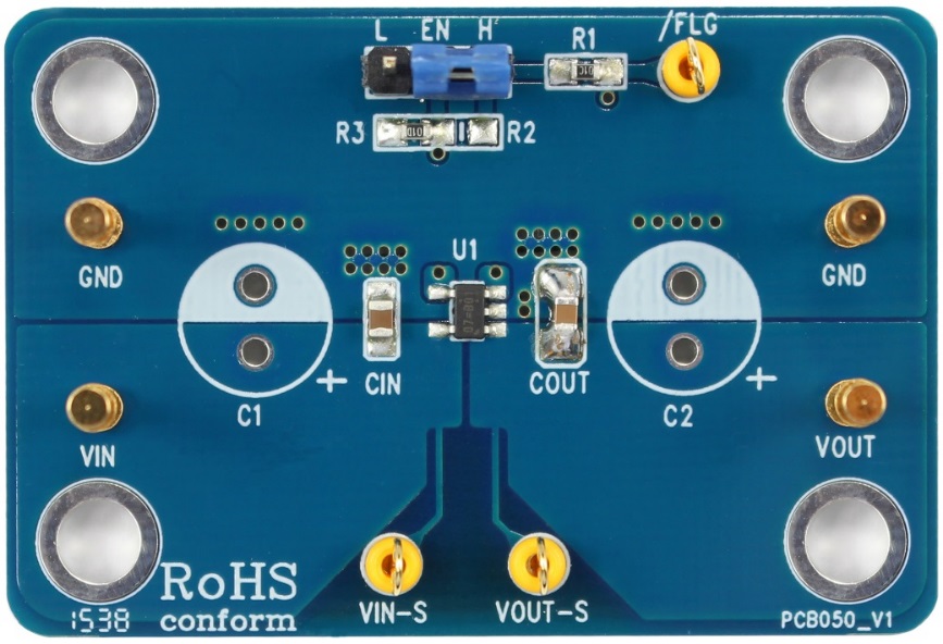
Please carefully inspect the EVB IC and external components, comparing them to the following Bill of Materials, to ensure that all components are installed and undamaged. If any components are missing or damaged during transportation, please contact the distributor or send e-mail to evb_service@richtek.com
Test Points
The EVB is provided with the test points and pin names listed in the table below.
|
Test point/
Pin name
|
Signal
|
Comment (expected waveforms or voltage levels on test points)
|
|
VIN
|
Input voltage
|
Power input. Support 2.7V to 6V Input Voltage.
|
|
EN
|
Enable test point
|
High = Enable. Apply a voltage exceeds than enable logic high voltage (2V) for chip enable.
|
|
GND
|
Ground
|
Ground.
|
|
VOUT
|
Output voltage
|
Output voltage pin. Probe this pin to observe the output voltage waveform.
|
|
/FLG
|
Fault FLAG Output
|
FLAG output indicator pin. FLAG is a low active output. Once the over current, short circuit, and over temperature occurring, it will indicate “LOW” after 10ms delay time.
|
Power-up & Measurement Procedure
1. Connecting input power (2.7V < VIN < 6V) and input ground to VIN and GND test pins respectively.
2. Connecting positive end and negative terminals of load to VOUT and GND test pins respectively.
3. There is a 3-pin header “EN” for enable control. To use a jumper at “HI” option to tie EN test pin to input power VIN for enabling the device. Inversely, to use a jumper at “LO” option to tie EN test pin and ground GND for disabling the device.
4. Connecting an external load up to 5A to the VOUT and GND terminals and verify the over current protection and FLAG indication.
Schematic, Bill of Materials & Board Layout
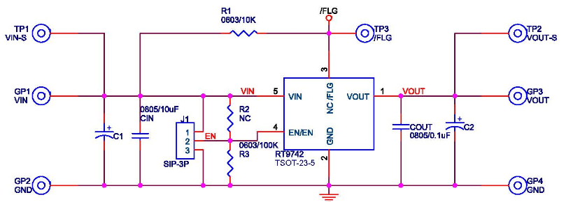
EVB Schematic Diagram
Bill of Materials
|
Reference
|
Qty
|
Part Number
|
Description
|
Package
|
Manufacture
|
|
U1
|
1
|
RT9742AGJ5F
|
Power Switch with Flag
|
TSOT-23-5 (FC)
|
RICHTEK
|
|
CIN
|
1
|
|
10µF/10V/X7R/0805
|
C-0805
|
|
|
COUT
|
1
|
|
0.1μF/50V/X7R/0805
|
C-0805
|
|
|
C1, C2
|
2
|
|
NC
|
|
|
|
J1
|
1
|
|
SIP-3P
|
SIP-3P
|
|
|
R1
|
1
|
|
10kΩ/0603
|
R-0603
|
|
|
R3
|
1
|
|
100kΩ/0603
|
R-0603
|
|
|
R2
|
1
|
|
NC
|
|
|
|
GP1, GP2, GP3, GP4
|
4
|
|
VIN, GND, VOUT, GND (Gold Pin)
|
SIP-1P
|
|
|
TP1, TP2, TP3
|
3
|
|
VIN-S, VOUT-S, /FLG (Test Pin)
|
SIP-1P
|
|
PCB Layout
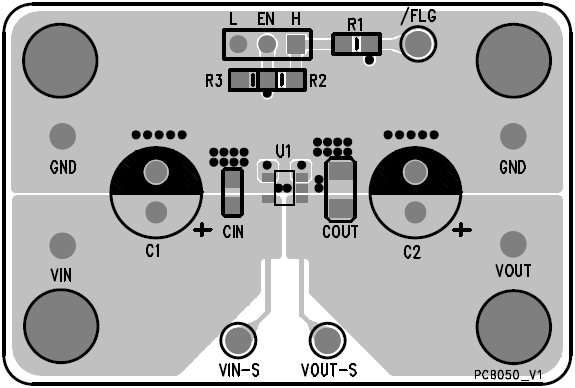
Top View
Bottom View