The Reduction of Input Voltage Spike on Power Switches
1. Introduction
The power switch is a low voltage, single N-Channel MOSFET
high-side power switch, optimized for self-powered and bus- powered Universal
Serial Bus (USB) applications.
In worse operating condition, an input voltage spike may
over the chip maximum input voltage specification to damage the chip. This
application note introduces solutions for reducing the input voltage spike on
power switches.
2. Power Switch Application Circuit
Figure 1 shows a typical application circuit of power switch.
There are two capacitors for input (Cin) and output (Cout). Flag pin is an open
drain output and one resistor (R1) is necessary for pull high resistor. The
power switch delivers power from input pin to output pin when EN pin is enabled.
The power switch features Enable control signal, Flag signal, over current protection,
short circuit protection, and thermal shutdown protection.
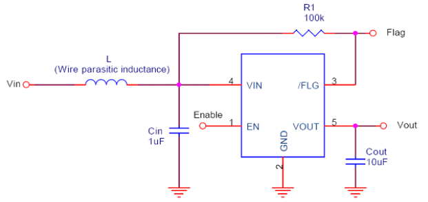
Figure 1. Typical application circuit
3. Input Voltage Spike
In steady state normal operation, the power switch delivers
a certain current from input power source to output pin and the voltage at VIN
pin almost equals to the input power source. However, when the power switch
is turned off suddenly, it will induce a spike voltage at VIN pin. The spike
voltage could be expressed as below.

Where L is the parasitic inductance of input wire between
power source and power switch input pin, di/dt is the change rate of input current.
If the spike voltage level exceeds the chip absolute maximum rated input
voltage, it may damage the chip.
Example 3-1
Figure 2 shows the
test result of RT9711 power switch operated in worse condition, input voltage
is set at maximum voltage 6.5V and input wire length is 35cm.
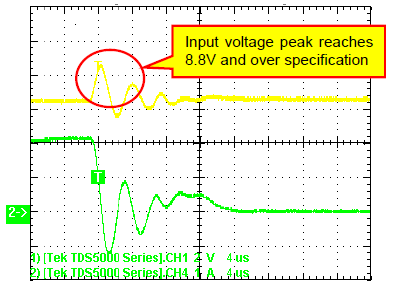
Figure 2. RT9711 power switch operated in worse condition:
Vin = 6.5V, Cin = 1μF, input wire length 35cm, (Vin_spike
= 8.8V)
When the output current is over maximum current rating,
the power switch limits the output current at OCP level (~2A in this case) and
decreases the output voltage so that the chip temperature raises up. Once the
chip temperature reach a certain over temperature protection (OTP) level, the
chip will turn off the power switch. So, the change of current in wire will
induce a spike voltage (Vin_spike) at the input pin. The test result shows that
the maximum voltage is 8.8V and it is over the absolute maximum rating of the
chip (6.5V). The chip may be damaged by the spike voltage.
4. Solutions for Reducing Input Voltage Spike
There are three recommendations to reduce the input
spike voltage shown as below.
4-1. Shorten the wire length between input
power source and power switch input pin.
4-2. Reduce the operating input
voltage level.
4-3. Increase the capacitance of input capacitor.
In the Example 3-1, if the input voltage changed from 6.5V to 5.5V and the
input wire length is changed from 35cm to 10cm, the spike voltage level will
be reduced greatly. Figure 3 shows the test result that the spike voltage (6.48V)
is under the absolute maximum rating (6.5V).
In most of applications, the
input voltage is 3.3V or 5V system. The power switch should be placed close
to the input power source to shorten the input wire length. To place a larger
input capacitor (ex: 33uF or larger) at the input pin is also a good solution.
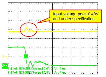
Figure 3. RT9711 power switch operated in condition:
Vin = 5.5V, Cin = 1μF, input wire length 10cm, (Vin_spike
= 6.48V)
5. Layout Consideration
In order to obtain better performance, careful PCB layout
is necessary. The following guidelines must be considered.
l Locate the input
capacitors as close as possible to the chip VIN pin and GND pin.
l Place
a ground plane under circuitry to lower both resistance and inductance.
l
Keep all power traces as short and wide as possible.
l Locate the output
capacitor as close to the connectors as possible to lower impedance between
the output port and the capacitor and improve transient load performance.
6. Conclusion
The input voltage spike could be controlled by the solutions
in section 4. It is necessary to take care on the operation conditions which
include operating input voltage level, input wire length between power source
and input pin, input capacitor, and PCB layout.