Analysis of Buck Converter Efficiency
Abstract
The synchronous buck circuit is wildly used to provide non-isolated power for low voltage and high current supply to system chip. To realize the power loss of synchronous buck converter and to improve efficiency is important for power designer. The application note introduces the analysis of buck converter efficiency and realizes major power component loss in synchronous buck converter.
Buck converter power loss analysis
To realize the power loss in converters is important for converter design optimization. Figure1 shows the general single phase synchronous buck converter circuit. The major power losses in synchronous buck converter circuit are listed as bellow :
A : Power semiconductor loss
B : Inductor loss
C : Driver loss
D : PCB trace loss
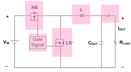
Figure 1. Synchronous buck converter
Power loss calculation
Low-power loss and highly efficient synchronous buck converters are in great demand for advanced micro-processors. The application note introduces and provides how to calculate the majority of power losses in a typical synchronous buck converter occur in the following components based on that the converter works in continuous conduction mode (CCM) fixed switching frequency, fixed input voltage and fixed output voltage.
A : Power semiconductor loss :
HMOS (High-Side MOSFET) summarizes to include : switching on & off and conduction loss.
LMOS (Low-Side MOSFET) summarizes to include : conduction, dead-time and reverse recovery charge loss.
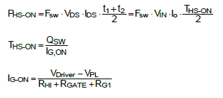
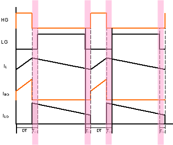
HMOS switching on loss :
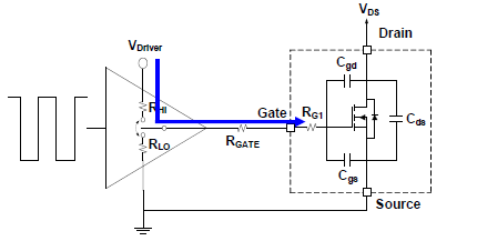
Figure 2. HMOS Driver switching on
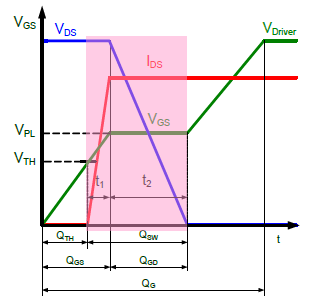
Figure 3. HMOS switching on loss area
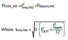
HMOS conduction loss :
The conduction loss of high-side MOSFET is determined by the on-resistances of the MOSFET and the transistor RMS current.
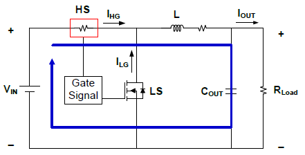
Figure 4. HMOS conduction on
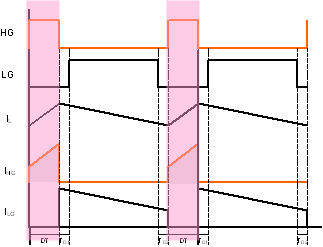
Figure 5. HMOS conduction on period
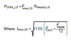
LMOS conduction loss :
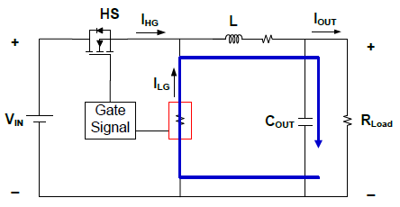
Figure 6. LMOS conduction on
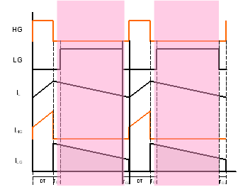
Figure 7. LMOS conduction on period
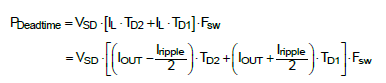
LMOS dead time body diode loss :
Dead-time loss is induced by LMOS body diode conduction during dead-times.
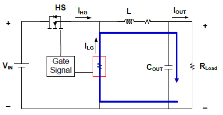
Figure 8. LMOS body diode conduction on
 :
:
Figure 9. LMOS body diode conduction on period
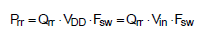
LMOS reverse recovery charge loss :
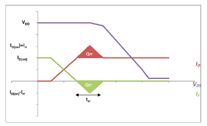
Figure 10. LMOS body diode reverse recovery period
B : Inductor DC & AC loss
Inductor DC loss :
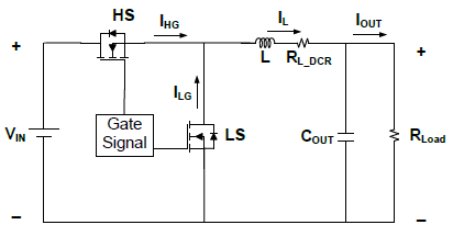
Figure 11. Current through inductor path
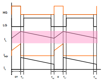
Figure 12. Inductor current path period
Inductor core loss :
Inductor core losses are major caused by an alternating magnetic field in the core material. The losses are a function of the operating frequency and the total magnetic flux swing. The core loss may vary from one magnetic material to another.
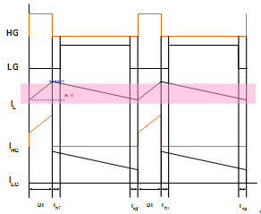
Figure 13. Inductor ripple current
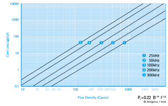
Figure 14. Core loss curve
The calculated and/or measured core loss is often directly provided by the inductor supplier. If not, a formula can be used to calculate the core loss as bellow :
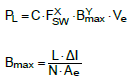
The PL is the power loss (mW),
Fsw : operating frequency
B : peak flux desity in Gauss
Ve : effective core volume
The specific value of C, X and Y are core loss parameters for each material
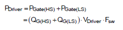
C: Gate driver loss :
The gate driver loss is straightforward given by MOSFET driver to charge /discharge total HMOS and LMOS Qg. The gate driver loss is depending on MOSFET total gate charge, driver voltage and Fsw.
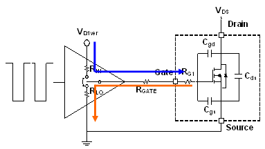
Figure 15. Driver turns on and off path
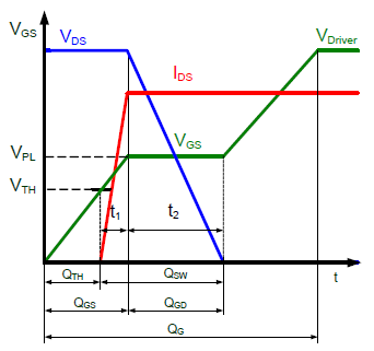
Figure 16. MOSFET driver on
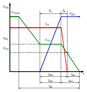
Figure 17. MOSFET driver off
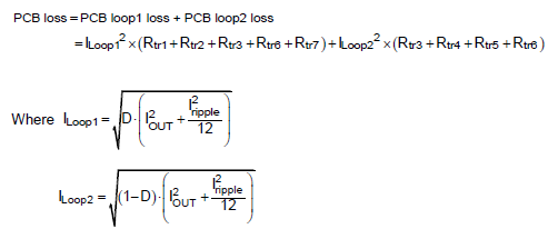
D : PCB loss :
Figure 18 could be illustrated as Figure 19 and Figure 20 with Rtr1~Rtr7 with loop1 (HMOS conduction) and loop2 (LMOS conduction) in detail.
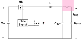
Figure 18. PCB trace diagram
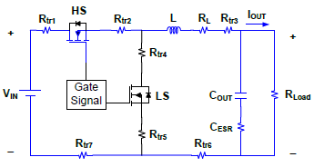
Figure 19. PCB loop1 trace
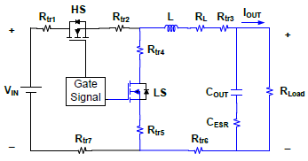
Figure 20. PCB loop2 trace
Power loss measurement and
calculation comparison
Although the buck converter power loss calculated equations are well introduced and documented. In order to check the accuracy of these power loss equations, Table1 shows the typical buck converter application parameter and Figure 21 illustrates the efficiency comparison between measurement and calculation.
Table 1. Buck converter application parameter
|
IC
|
RT8120
|
|
VIN
|
12V
|
|
Vout
|
1.2V
|
|
FSW
|
300kHz
|
|
VDD
|
12V
|
|
L
|
1mH
|
|
DCR
|
1.2mW
|
|
HMOS
|
BSC090N03LS
|
|
LMOS
|
BSC090N03LS*2
|
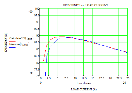
Figure 21. Measurement and calculation of efficiency comparison
Figure 22 shows the key component loss in buck converter including HMOS, LMOS, inductor, driver and PCB trace loss. Readers can check what the major loss contributed in each system loading.
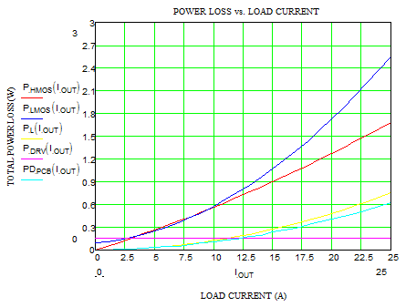
Figure 22. Key component loss in buck converter
Figure 23 shows detail component loss in buck converter and illustrates the loss v.s Iout in the curve.
HMOS : PHSW (Switching loss) and PHCOD (Conduction loss)
LMOS : PLCOD (Conduction loss), PL_DIODE (Dead-time body diode loss) and PRR (Reverse recovery loss)
Inductor : PL (Inductor DC & core loss)
Driver : PDRV (Gate driver charge loss)
PCB : PPCB (PCB trace loss)
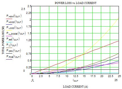
Figure 23. Detail power loss in buck converter
Conclusion
This application document analyzes power loss in synchronous buck converters and presents the detailed calculations for each part of the power loss. The loss calculation also compares with real buck converter measurement and provides the key component loss data to consider how to improve the buck converter efficiency for component and PCB plane consideration.