How to Eliminate Over Stress of MOSFET during Start-up of Flyback Converter
Abstract
This application note investigates “how to effectively eliminate over-stress
of MOSFET during start-up of flyback converters” in three major aspects: first,
the design of flyback controllers with the Richtek proprietary embedded soft-start
function; next, the relationship between feedback stability of the system and
stress of switching MOSFETs; finally, analysis and design of a passive voltage
clamp RCD Snubber. When developing power supply systems, R&D engineers can
refer to this note on how to reduce stress of switching MOSFETs to prevent them
from being damaged, and also to enhance reliability of circuit operation.
1. Introduction
Switching Power Supply, compared to Linear Power Supply, is widely used due
to its advantages, such as small size, light weight, high efficiency, etc. Flyback
Converter, one of the switching power supply topologies, is most suitable for
power supply systems that are below 150W because of its unique features of isolation
between primary and secondary sides, simple circuit architecture, few components,
low cost, etc.
Since switching power MOSFETs play a very important role in switching power
supply converters, how to effectively eliminate over-stress of MOSFET during
the start-up of flyback converters will be the main focus to be discussed in
this application note. The three major aspects to be investigated are flyback
controller design, feedback stability, and Snubber design.
2. Flyback Controller Design—Richtek Proprietary Embedded Soft Start Function
Figure 1 is a circuit diagram of a typical flyback converter. Richtek RT7736
– SmartJitter PWM flyback controller is taken as an example. The functional
block diagram, from the RT7736 datasheet, is shown in Figure 2. When VDD goes
up and exceeds the threshold voltage (VTH_ON) of the controller IC
RT7736, the controller will start to operate and Soft Start (SS) function will
be activated immediately.
The oscillator, built in the controller IC, generates a clock to set the
S pin of an S-R Flip-Flop. The voltage (VCS) across the current sense
resistor (RCS) will compare with the lower value between the feedback
voltage (VCOMP) and the current limit signal (VCS_CL)
from Constant Power block. If VCS exceeds the lower value between
them, the PWM comparator output will reset the S-R Flip-Flop and then the pulse
width of VGATE is thus determined.
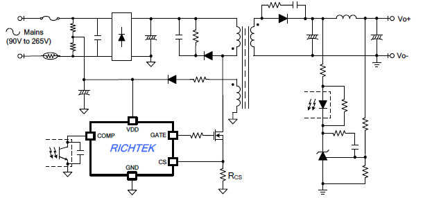
Figure 1. A circuit diagram of a typical flyback converter
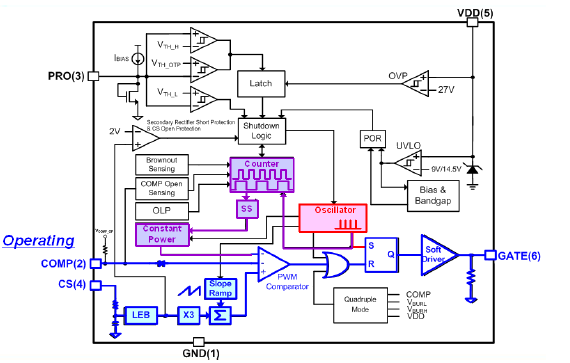
Figure 2. The functional block diagram of RT7736
A flyback controller IC controls the switching transistor (Ex: MOSFET) of
a flyback converter via the GATE pin. When the switching MOSFET turns ON or
closes, the input voltage is completely across the transformer (coupled inductors)
so the inductor current increases linearly and thus the energy stored in the
inductor gradually increases. On the other hand, since the power diode is reverse-biased
at this stage, it is the output capacitor that supplies the energy to the output
load. With the feedback control signals, the gate drive signal (VGATE)
can be set to turn off the switching MOSFET. Once the MOSFET is switched OFF,
due to the continuity of the magnetic flux of an inductor, the power diode is
forced ON, and the inductor voltage will inversely induce the magnetic flux.
The inductor current now flows through the diode, and decreases linearly. This
current will supply the output load and also charge the output capacitor until
the next cycle is triggered by the internal clock of the controller IC. The
switching operation of a flyback converter will be repeated every clock cycle
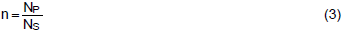
in such pattern. Figure 3 illustrates how a flyback converter and its controller
operate in continuous conduction mode (CCM).
When the switching MOSFET is turned ON, the rising slope (mR)
of the voltage (VCS) on the current sense resistor is as:
When the switching MOSFET is turned OFF, the falling slope (mF) of the voltage
(VCS) on the current sense resistor is as:
where VIN is the input voltage across the transformer; LP
is the primary-side magnetizing inductance of the transformer; VO
is output voltage; VF is the forward voltage of the power diode;
n is the turns ratio of the transformer; NP is the primary-side number
of coil turns of the transformer; NS is the secondary-side number
of coil turns of the transformer.
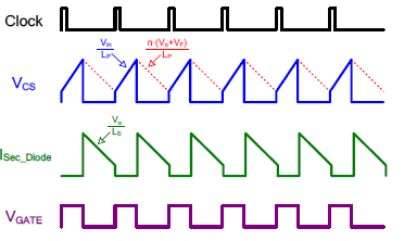
Figure 3. The diagram shows how the flyback converter and its controller
operate in CCM
When a flyback converter just starts up, the output voltage is still zero,
and has not been built up yet. From equation (2), it can be seen that the falling
slope of the current sense resistor voltage (VCS) is close to zero,
too. Since the controller IC will turn on the switching MOSFET for at least
a minimum ON time (TON_MIN), VCS will keep rising. Henceforth, peak
current of the MOSFET will continue to increase with every cycle. The moment
the MOSFET is switched OFF, the accumulated peak current, the leakage inductor
of the transformer, and the parasitic capacitor of the MOSFET can cause a high
frequency oscillation, which then induce a huge voltage spike across drain and
source (VDS) of the MOSFET. Therefore, during start-up of a flyback
converter, under high line input voltage condition, the over-stress problem
of the switching MOSFET will arise, as shown in Figure 4(a). Besides, when the
output of a flyback converter is short and then auto recovery protection will
be triggered by the controller IC, the stress of the MOSFET will become even
worse under high line input voltage condition, as shown in Figure 4(b).
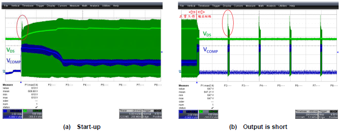
Figure 4. The stresses of the switching MOSFET of a flyback converter
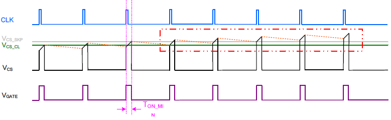
The Richtek proprietary embedded soft start function, incorporated in the
RT7736 – SmartJitter PWM flyback controller, can effectively suppress peak current
during start-up to enhance reliability of circuit operation, and also allow
the lower rated voltage and current for switching power MOSFET. The proprietary
embedded soft start function will be activated first when the controller IC
starts to operate. With the features of a stepped current limit signal as well
as overcurrent threshold voltage (VCS_SKP) and cycle skipping mode,
step by step, output voltage can be slowly built up. During soft start, when
the voltage on the current sense resistor (VCS) exceeds overcurrent
threshold voltage (VCS_SKP), the controller IC will enter cycle skipping
mode. Since the cycle is skipped, this allows more time for the inductor voltage
to induce inverse magnetic flux. Thus, peak current of the switching MOSFET
can be reduced, and the pulse width of the gate voltage (VGATE) for
the next cycle can be wider than Minimum On Time (TON_MIN) so that
the output voltage can be built up more efficiently. Figure 5 illustrates how
the Richtek proprietary embedded soft start function works. Figure 6 shows the
comparison between conventional soft start and the Richtek proprietary embedded
soft start function -- cycle skipping mode.
Figure 5. The diagram of the Richtek proprietary embedded soft start function
(a) Conventional soft start function
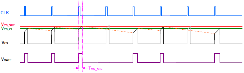
(b)RICHTEK proprietary soft start function – cycle skipping mode
Figure 6. Conventional vs. RICHTEK proprietary soft start function
The same flyback converter power supply system is used for experiments, which
are to measure the stress during start-up of the system. Figure 7 shows the
comparison between conventional soft start function and the Richtek proprietary
soft start function on the same flyback converter after power on. A high voltage
spike is seen on the system with a conventional soft start function right after
power on. When the output voltage is gradually established, such that the magnetizing
flux of the inductor and the inverse magnetic flux induced by the inductor voltage
will be close, the stress of the switching MOSFET is reduced gradually. When
eventually the output voltage is completely built up, the maximum voltage stress
(VDS_MAX) of the switching MOSFET will also be reached.
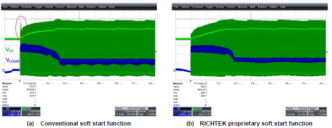
Figure 7. The stress of MOSFET during start-up-Conventional soft start function
vs. RICHTEK proprietary soft start function
The same flyback converter power supply system is used for experiments, which
are to measure the stress when the output of the system is short. Figure 8 shows
the comparison between conventional soft start function and RICHTEK proprietary
soft start function on the same flyback converter during output short. When
the output of a flyback converter is short and then auto recovery protection
will be triggered by the controller IC, the stress of the MOSFET will become
even worse under high line input voltage condition. The optimized Richtek proprietary
soft start function with output short protection can effectively reduce stress
of switching MOSFETs so that they can be prevented from damage to enhance reliability
of circuit operation.
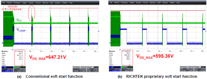
Figure 8. The stress of MOSFET during output short – conventional soft start
function vs. RICHTEK proprietary soft start function
3. Flyback Converter –Relationship between Feedback Stability and Stress of MOSFET
In the design of flyback converters, the turns ratio (n) of the transformer
is directly related to voltage stress of MOSFETs. In other words, the maximum
duty cycle determines the turns ratio of the transformer, which then decides
voltage stress of MOSFET.
The maximum voltage stress of the switching MOSFET
(VDS_MAX) is as below:

where Vin_max is the maximum input voltage across the transformer;
n is the turns ratio of the transformer; VO is the output voltage;
VF is the forward voltage of the power diode; VSpike is
voltage spike caused by the leakage inductance of the transformer (will be explained
later).
According to the operating principle of converters, the duty cycle can be
seen as the ON-Time ratio of switching MOSFET and Diode. From the viewpoint
of effective semiconductor utilization, the condition that either one has half
duty cycle can achieve the highest utilization rate. In other words, the maximum
duty cycle (Dmax) is set at around 0.5 to have the highest utilization
rate for MOSFET and Diode. Therefore, Duty Cycle is normally set at 0.5 at the
lowest input voltage. Then calculate the turns ratio (n) of the transformer
and adjust n and Dmax, based on voltage stress margins of MOSFET
and Diode. For details about how to determine turns ratios of transformers in
flyback converters, please refer to the application note of “Design Guide for
Fixed-Frequency Flyback Converter.” However, “Flyback Converter – the Relationship
between Feedback Stability and Stress of MOSFET”, which is often neglected by
designers, will be discussed in this application note, while assuming the flyback
converter and the turns ratio of its transformer have been optimized.
To investigate feedback stability of the flyback converter, the existing
RHP zero of the flyback converter must be first understood. This zero cannot
be compensated with the conventional pole, so the cross-over frequency (fc)
must be set far below this RHP zero. Practically, the cross-over frequency is
usually set below 3kHz. For an off-line flyback converter, it is most appropriate
to set cross-over frequency in the range of 800Hz to 3kHz, and phase margin
(ψm) > 45° under the condition of low line and full load, given
65kHz as the switching frequency. Please refer to the application note of “Feedback
Control Design of Off-line Flyback Converter” for the details about feedback
design of flyback converters.
With different compensation designs for feedback stability, the same flyback
converter power supply system is used for experiments to measure stress of MOSFET
and to prove the theoretical analysis. Two feedback compensation designs, fc <
800 Hz & ψm < 45° vs. fc > 800 Hz & ψm >
45°, are examined for the relationship between feedback stability and stress
of the MOSFET. Figure 9 and 10 show the measurements of cross-over frequency
and phase margin of the loop gain under the conditions of low line and high
line, respectively, both with full load. Referring to Figure 11 for stress of
MOSFET of the flyback converter under the condition of high line and full load,
it can be seen that with lower cross-over frequency and insufficient phase margin,
the transient response is slower, which causes the overshoot when output voltage
is built-up. From equation (4), it can be seen that the overshoot of the output
voltage will increase stress of the switching MOSFET. Therefore, with careful
design of cross-over frequency and phase margin to achieve better feedback stability
compensation, stress of the MOSFET of a flyback converter during start-up can
be effectively reduced, which can thus prevent MOSFET from damage.
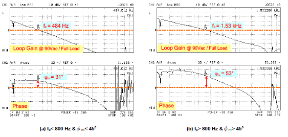
Figure 9. Cross-over frequency and phase margin of the loop gain under low
line and full load
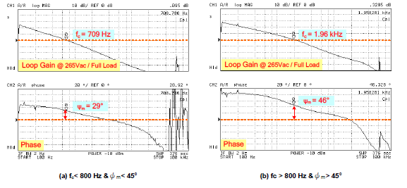
Figure 10. Cross-over frequency and phase margin of the loop gain under high
line and full load
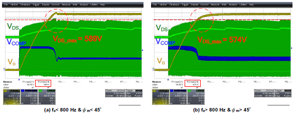
Figure 11. Stress of the MOSFET of the flyback converter under high line
and full load
4. Analysis and Design of a Passive Voltage Clamp RCD Snubber
Since the leakage inductor of a transformer and the parasitic capacitor of
a MOSFET of a Flyback converter exist, Figure 12 depicts the equivalent circuit
model of a flyback converter as well as these elements. When the MOSFET turns
OFF or opens, because the magnetic flux of an inductor must be continuous and
the magnetic flux stored in the leakage inductor cannot be transferred to the
secondary side, the leakage inductor current is cut off immediately, which causes
a high voltage spike across the drain and source of the MOSFET (VDS).
The resonance caused by the leakage inductor of the transformer and the parasitic
capacitor of the MOSFET triggers high-frequency oscillation, as shown in Figure
13. Figure 13(a) shows a flyback converter operates in continuous conduction
mode (CCM), and Figure 13(b) in discontinuous conduction mode (DCM).
The high-frequency oscillation, triggered by the resonance caused by the
leakage inductor of the transformer and the parasitic capacitor of the MOSFET,
is superimposed on the drain/source voltage (VDS) of the MOSFET.
The superimposed voltage spike (VDS_Peak) is as below:
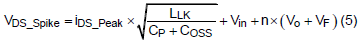
where iDS_Peak is the peak current through the MOSFET, from the
primary side of the transformer; LLK is the primary-side equivalent
leakage inductor of the transformer; CP is the primary-side equivalent
parasitic capacitance of the transformer; COSS is the MOSFET parasitic
output capacitance; Vin is the input voltage across the transformer;
n is the turns ratio of the transformer; VO is the output voltage;
VF is the forward voltage of the power diode.
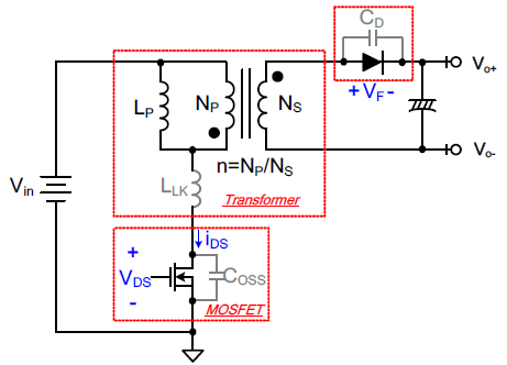
Figure 12. A flyback converter and the equivalent circuit model
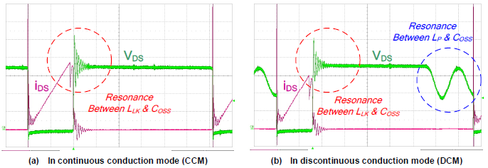
Figure 13. The waveforms show the resonance caused by the parasitic leakage
inductance and capacitance from the elements of a flyback converter
The voltage spike, caused by the parasitic inductor and capacitor of the
components, and the resulting high-frequency oscillation will cause great stress
and even damage to the switching MOSFET. High-frequency oscillation may also
induce EMI noises to the power supply system and result in reliability problem
for the circuits. An appropriate Snubber can be added to suppress this high-frequency
oscillation so that the problems mentioned above can be effectively resolved.
A passive voltage clamp RCD Snubber, which is now widely adopted in flyback
converters, is introduced in this application note and is depicted in Figure
14. The moment when the switching MOSFET turns OFF, the magnetic flux of the
inductor must be continuous, so the leakage inductor current of the transformer
continues to flow in the original direction. However, this current will flow
into two paths; one path (iDS) is through the gradually switching-off
MOSFET and the other (iSn) is through the diode of the Snubber to
charge the capacitor (CSn). Since the voltage on CSn cannot
change abruptly, the rising rate of the MOSFET voltage is then reduced. Besides,
the original switching-off power dissipation of the MOSFET now gets to transfer
to the Snubber. Figure 15 shows the voltage and current waveforms of a passive
voltage clamp RCD Snubber, operating in discontinuous conduction mode (DCM).
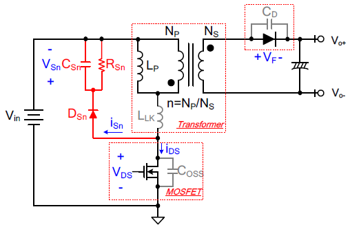
Figure 14. A flyback converter with a passive voltage clamp RCD snubber circuit
added
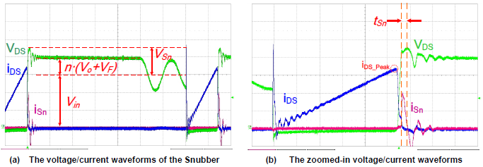
Figure 15. The voltage and current waveforms of a passive voltage clamp RCD
Snubber (DCM)
The moment the MOSFET turns OFF, the diode of the Snubber
turns ON. The rising slope (mi_Sn) of the leakage inductor current
of the transformer is as below:
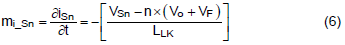
where iSn is the current through the diode of
the Snubber.
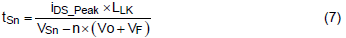
The ON-time (tSn) of the diode of the Snubber is
as below:
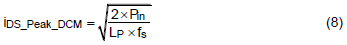
According to different modes of operation, peak current (iDS_Peak)
of a flyback converter can be differentiated as:
Peak current (iDS_Peak_DCM) of the switching MOSFET, operating
in discontinuous conduction mode, is as below:
Peak current of the switching MOSFET, operating in continuous conduction
mode (iDS_Peak_CCM), is as below:

where Pin is the input power of a flyback converter.
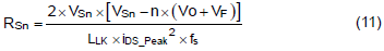
Power dissipation of the Snubber (PSn) is as below:

where the capacitor voltage (VSn) is usually set as 2~2.5 times
of n×(VO + VF).
Take equation (10) into Electric Power Formula, the resistor value (RSn)
of the Snubber can be obtained:
The voltage ripple (ΔVSn) of the capacitor (CSn) of
the Snubber is usually set as 5~10% of the capacitor voltage (VSn).
Based on Volt-Second Balance Principle, the capacitor value (CSn)
of the Snubber can be derived, as below:
The maximum drain-source voltage (VDS) of the switching MOSFET
in a flyback converter usually occurs when the system operates at the highest
input voltage and full load condition. Therefore, it can be used as a design
condition to find the capacitor and resistor values in the design of the passive
voltage clamp RCD Snubber for a flyback converter. As for the diode in the Snubber,
a fast diode is the typical choice. Figure 16 shows the comparison of the stress
on the switching MOSFET of the same flyback converter power supply system, with
and without a passive voltage clamp RCD Snubber. An optimized passive voltage
clamp RCD Snubber can effectively reduce stress of MOSFET to prevent damage
and to enhance reliability of circuit operation, and also to improve the EMI
problem induced by high-frequency oscillation.
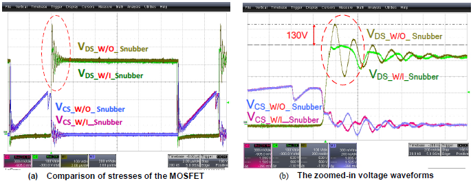
Figure 16. Comparison of the stress of the MOSFET, with vs. without a passive
voltage clamp RCD Snubber
5. Conclusion
Power MOSFETs, switching components, play an important role in switching
power converters. Flyback converters have the features of isolation between
primary and secondary sides, simple circuit architecture, few components, and
low cost, etc. so that they are widely used. The maximum stress of the MOSFET
in a flyback converter does not necessarily occur when operating at steady state
with full load. Instead, start-up time of a flyback converter is what to be
carefully examined. This application note provides the theoretical explanation,
verified by the experiment results, and investigates “how to effectively eliminate
over-stress of MOSFET during start-up of flyback converter” comprehensively
in many different aspects: they are from the core of the system – the soft start
function of a flyback controller IC, the system level – feedback stability compensation
of a power system, finally to the added application circuit – analysis and design
of a passive voltage clamp RCD Snubber. It aims to provide R & D engineers
with a good reference on how to reduce stress of the MOSFET to prevent damage
and to enhance reliability of circuit operation in the development and design
of a flyback converter power supply system.