DCR Temperature Compensation
Abstract
The DCR current sensing technique provides a good solution to get the inductor current information due to its lossless characteristic. However, the inductor DCR value may vary with the temperature, since copper is a positive temperature coefficient. Therefore, the temperature variation on the DCR value may cause the controller to sense a false current signal. To cancel the temperature effect, a DCR temperature network is usually added in the current sense loop. This application note will introduce the basic concept and the implementation methods for DCR temperature compensation.
1. Why We Need a DCR Temperature
Compensation Network
Figure 1 shows the DCR current sensing network. When the time constants are equal, that is, CxRx = L / DCR, the VCX voltage can be used to obtain the inductor current signal as shown in (1). However, the DCR value will increase proportionally with the temperature, which is described in (2) where the parameter TCDCR is the temperature coefficient of the copper with a positive value. When the circuit operates in the heavy load condition, the inductor’s temperature will increase as well. That will make the regulator falsely detect the load current level and provide the inaccuracy current reporting information because the DCR value varies under different temperature conditions. Besides, the output voltage could not reach to its desired value and then violate the load-line specs while adaptive voltage position droop for Vcore applications is required. Therefore, a temperature compensation network is used to solve the problem.
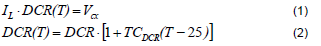
Figure 1. DCR current sensing network
2. Topologies of DCR Temperature
Compensation
The DCR temperature compensation network aims the DCR value to be invariant with the temperature, hence the VCX voltage can be only dependent on the inductor current. Since the DCR is a resistor with the positive temperature coefficient, a resistor network with the negative temperature coefficient should be inserted in the current sensing loop to compensate the DCR variations due to temperatures. When there are Y temperature points need to be compensated, the compensation network requires Y resistors and one negative temperature coefficient (NTC) thermistor to cancel out the DCR variations under these Y temperature points. However, according to the current sensing topologies, the DCR temperature compensation network should be implemented in the proper place. Figure 2 and Figure 3 are respectively shown the implementation of the temperature compensation network in the sum current and differential sensing topologies. Therefore, the sum current sensing topology demonstrates the compensation network which is used to compensate three temperature points, and the differential sensing topology demonstrates the compensation network for two temperature points. Equations (3) and (4) are used to describe the design criterions for these two current sensing topologies.
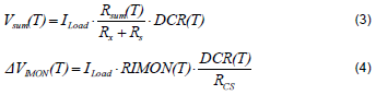
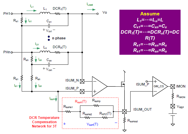
Figure 2. DCR temperature compensation network in sum current sensing topology
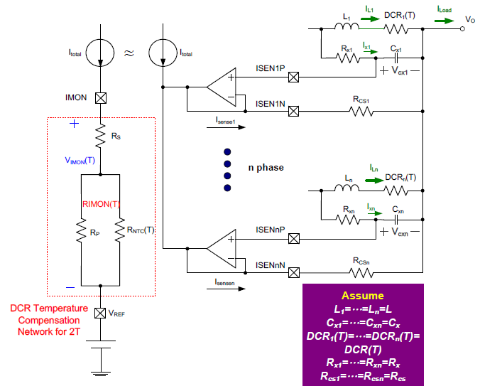
Figure 3. DCR temperature compensation network in differential current sensing topology
3. Derivation of DCR Temperature
Compensation Network
In this section, the sum current sensing topology will be used as an example to derive the temperature compensation network. As shown in (3), the load current information can be correctly acquired through the Vsum voltage with a proper gain. This gain can be expressed as the ratio between Rsum and (Rx+Rs) and be shown in (5). For example, this ratio in RT8893 must set as 4 for the proper operation.
However, in order to cancel the temperature effect on the DCR, a NTC thermistor is inserted in the Rsum network to make the Vsum voltage be invariant with the temperature. The relationship between NTC and temperature is shown in (6), where β is the temperature coefficient of the NTC thermistor and is varied with different NTC thermistor.
If there are three temperature points (TL, TR, TH) need to be compensated, the Vsum voltage at these three temperature points should be set equally and the results can then be shown in (7). Rsum(T) is the equivalent resistor of the thermal compensation network with a NTC thermistor and can be obtained as (8).
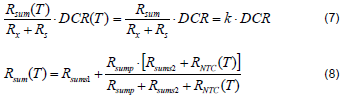
Therefore, with above equations, the parameters of the Rsum network can be accordingly found out as (9), (10), and (11). Please see Appendix I for further details.
where
After implementing the temperature compensation, the VSUM error at these three temperature points (ex: 20°C, 60°C, and 100°C) should be zero as shown in Figure 4.
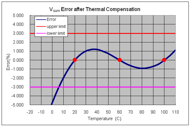
Figure 4. Vsum error after DCR temperature compensation
4. Design Example of DCR Thermal
Compensation Network
The following design approach will use the sum current sensing topology with RT8893 as an example, and the specifications are designed to meet the Intel VR12.5 requirements.
|
VCORE Specification
|
|
Input Voltage
|
10.8V to 13.2V
|
|
Number of Phases
|
3
|
|
Vboot
|
1.7V
|
|
VDAC(MAX)
|
1.8V
|
|
ICCMAX
|
90A
|
|
ICC-DY
|
60A
|
|
ICC-TDC
|
55A
|
|
Load Line
|
1.5mΩ
|
|
Fast Slew Rate
|
12.5mV/μs
|
|
Max Switching Frequency
|
300kHz
|
In Shark Bay VRTB Guideline for desktop platform, the requirements of the output filter are as follows:
Output Inductor: 360nH/0.72mΩ
Output Bulk Capacitor: 560μF/2.5V/5mΩ(max) 4 to 5pcs
Output Ceramic Capacitor: 22μF/0805 (18pcs max sites on top side)
Step 1 : Determine the Parameters of Inductor
Determine inductor value.
Output inductor: 360nH/0.72mΩ
Determine DCR temperature coefficient TCDCR.
TCDCR = 3930ppm
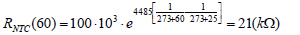
Therefore, the inductor DCR value with temperature effect can be calculated by using (2). The following calculation result gives an example of the DCR value at 60°C.

Step 2 : Determine NTC Parameter for Thermal Compensation
Using NCP15WL104J03RC as a NTC thermistor, the resistance is 100kΩ and the β value is 4485. By using (6), the NTC resistance at different temperature can be calculated. When a NTC thermistor operates at 60°C, the resistance can then be calculated as follows:
Step 3 : Design DCR Current Sensing Network and Rx, Rs and Rsum Values
DCR current sensing capacitor Cx and the resistance of RX and RS can be determined from the application note of DCR Current Sensing Topology.
Cx = 1μF, Rs = 3.41kΩ, and Rx = 590Ω
In RT8893, the ratio between Rsum and (Rx+Rs) must set as 4 for the proper operation.
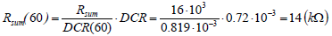
Rsum = 4•(Rx+Rs) = 16kΩ
Step 4 : Design Rsum Resistor Network
Set three temperature points for thermal compensation.
Choose (TH, TR,TL) = (100, 60, 20)
For example, the Rsum value at 60°C can be obtained from (7):
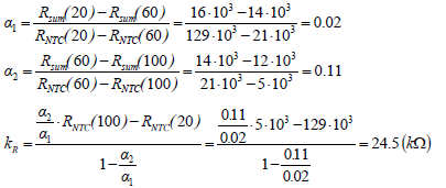
Therefore, the parameters α1, α2, and KR can then be calculated as follows:
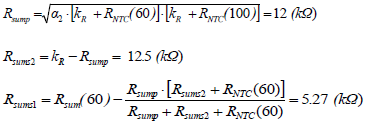
Use (9), (10), and (11), the Rsump, Rsums2, and Rsums1 can be found accordingly.
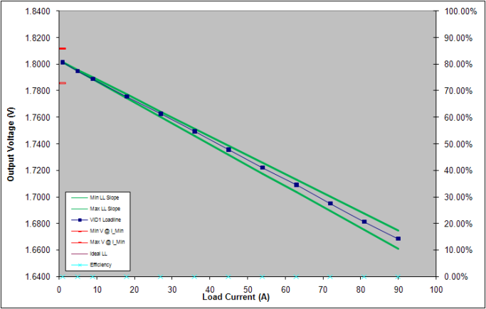
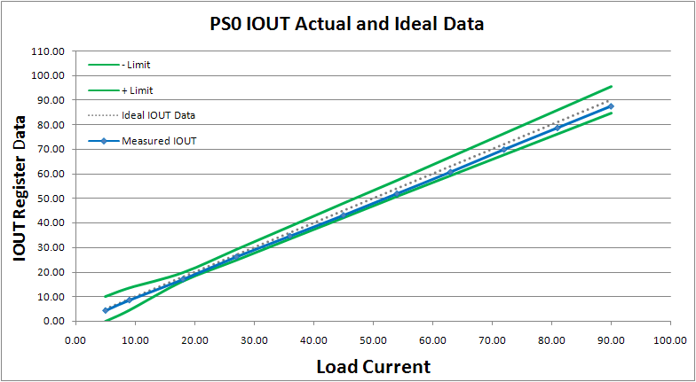
5. Experiment Result
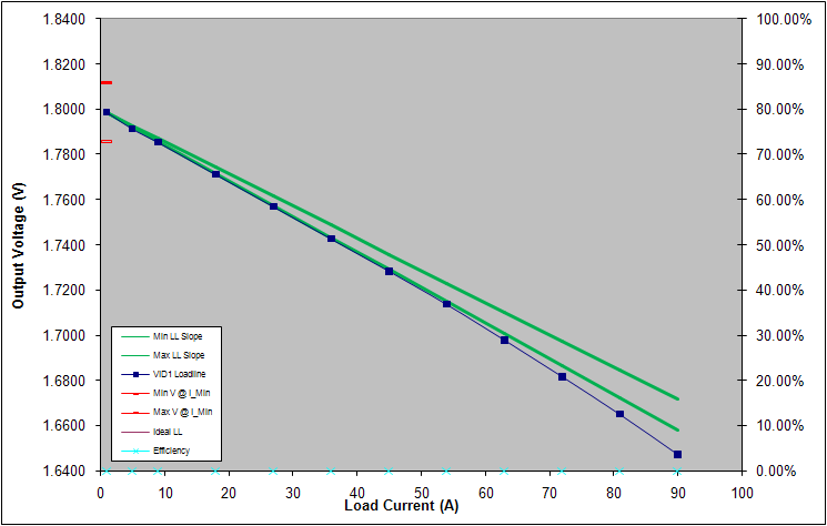
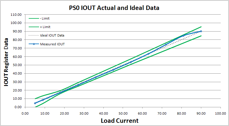
Figure 5 shows the DCLL and DIMON reporting with DCR temperature compensation. From the experiment results, the DCLL and DIMON reporting are both inside the tolerance band. However, without DCR temperature compensation, the overestimated DIMON reporting result in the heavy load condition will cause DCLL to violate the load line specs as shown in Figure 6.
(a) DCLL
(b)DIMON reporting
Figure 5. DCLL and DIMON reporting results with DCR temperature compensation
(a) DCLL
(b)DIMON reporting
Figure 6. DCLL and DIMON reporting results without DCR temperature compensation
6. Conclusion
This application note provided the implementation methods and useful design equations for DCR temperature compensation. With proper design procedure, it can effectively mitigate the temperature variation on DCR values and provide correct current information for DCR current sensing applications.
7. Reference
[1] Richtek, RT8884B datasheet.
[2] Richtek, RT8893 datasheet.
[3] Intel, VR12.5 Pulse Width Modulation (PWM) Specification
[4] Richtek, DCR Current Sensing Topology Application Note.
Appendix I Derivation of DCR Temperature Compensation
Network
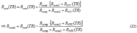
Substitute three temperature points (TL, TR, TH) into (8), (12) to (14) can be obtained. Therefore, (15) and (16) can be respectively obtained from (12)–(13) and (13)–(14).
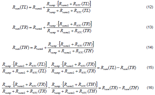
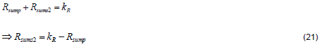
Define kR=Rsump+Rsums2, (15) and (16) can be further expressed as (17) and (18).
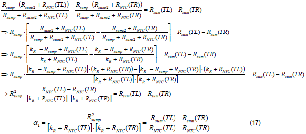
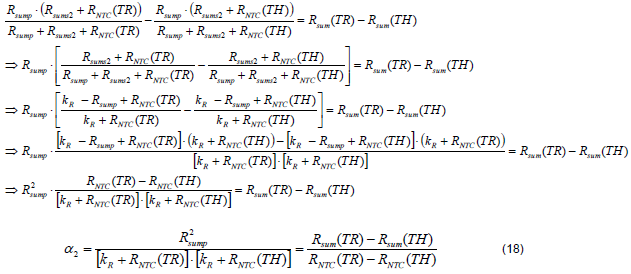
Equation (19) can be derived by (18)/(17).
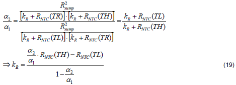
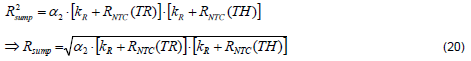
From (18), the Rsump can be found as shown in (20).
Then, the Rsums2 can be obtained as (21).
Therefore, the Rsums1 can be derived as (22).