Non-conformant Product Return Handbook
In order to enhance data analysis efficiency and increase failure analysis success rate, Richtek defines a guideline for returning the non-conformant products.
Please follow the guideline and contact your Richtek FAE, Sales or Distributors for the file.
Customer Complaint Notice (CCN) Guidelines
When customers want to return the failure sample to Richtek for future analysis, please contact the Richtek sales/FAE/agent to apply the "Customer Complaint Notice and Engineering Supporting Notice" (PQA012-01-5) and follow the CCN guidelines below to provide the detailed information.
| Category |
Provided by Customer Side |
| Failure information |
- Provide the failure rate, failure stage and failure symptom information.
- Take a picture of reel label information (including date code/lot ID etc.).
|
| Sample status |
- Reserve appearance integrity and provide clear pictures (top side and bottom side).
- Except for Richtek requirement, the returned sample needs be de-mounted from PCBA at customer side.
|
| Electrical status |
- Provide the test conditions and test results of the failure sample. (For example: VIN/VOUT/Frequency conditions, power on/off sequence, application circuit condition, leakage current level or abnormal waveform etc.)
- Check the resistance of abnormal pin and compare it with good sample by multi-meter.
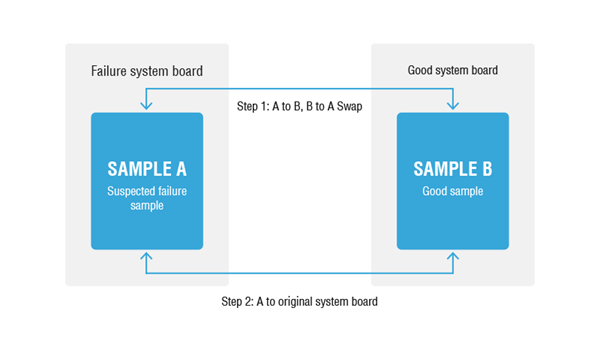
- Provide A-B-A Swap result to make sure the failure symptom is related to Richtek component.
|
| Sample transportation |
- Place the returned sample in a safety container to protect it from ESD or physical damage during transportation.
|
Product Analysis Notice
To achieve effective quality analysis and valuable analysis results, Richtek does not accept the following faulty products to be returned for Richtek analysis.
1. The chip has been seriously damaged. (For example: die surface appearance burnt-out, lead/ package are severely bent or broken, die chipping/crack etc.)
2. Excessive solder residue or abnormal coating material remaining on the pins or BGA.
3. Richtek is not responsible for cleaning the customer's solder residual, underfill or coating, so customer should ensure that the samples to be returned are in a testable status. (such as ATE test)
Electrical Over Stress (EOS) Notice
The damage caused by serious electrical over stress (EOS) will cover up the real problem. Richtek does not understand the customer's operation, environment, temperature and other conditions when the failure occurs. Thus, Richtek is not responsible for speculating the root cause of excessive electrical stress, and will not be pursued for any effective actions.