Purpose
The RT8498 is specifically designed to be operated in Buck,
Boost and Buck-Boost converter applications. This document explains the function
and use of the RT8498 evaluation board (EVB), and provides information to enable
operation, modification of the evaluation board and circuit to suit individual
requirements.
Introduction
General Product Information
The RT8498 is a current-mode LED driver supporting wide input
voltage range from 3V to 18V and output voltage up to 18V. With internal 350kHz
operating frequency, the size of the external PWM inductor and input/output
capacitors can be minimized. High efficiency is achieved by a 100mV current
sensing control. LED dimming control can be done from either analog or PWM signal.
The RT8498 provides an internal soft-start function to avoid inrush current
and thermal shutdown to prevent the device from overheat. The RT8498 is available
in the SOT-23-6 package.
Product Feature
- High Voltage : VIN Up to 18V, VOUT Up to 18V
- Built-In 2A Power Switch
- Current-Mode PWM Control
- 350kHz Fixed Switching Frequency
- Analog, PWM Digital or PWM Converting to Analog with One External Capacitor
- Internal Soft-Start to Avoid Inrush Current
- Under-Voltage Lockout
- Internal Over Voltage Protection to Limit Output Voltage
- Cycle-by Cycle Current Limit
- Thermal Shutdown
Key Performance Summary Table
|
Key Features
|
Evaluation Board Number: PCB082_V1
|
|
Default Input Voltage
|
4.5V to 18V
|
|
Max Output Current
|
1A
|
|
Default Output Voltage
|
3.0V
|
|
Default Marking & Package
Type
|
RT8498GE, SOT-23-6
|
|
Operation Frequency
|
Steady 350kHz at all loads
|
Bench Test Setup Conditions
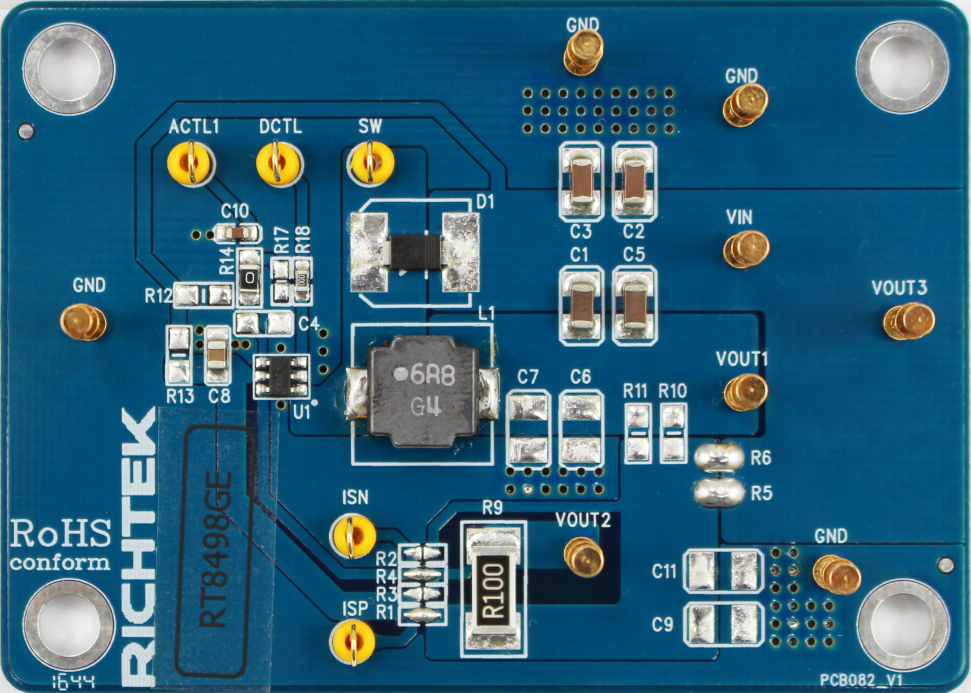
Headers Description and Placement
Carefully inspect all the components used in the EVB according
to the following Bill of Materials table, and then make sure all the components
are undamaged and correctly installed. If there is any missing or damaged component,
which may occur during transportation, please contact our distributors or e-mail
us at evb_service@richtek.com.
Test Points
The EVB is provided with the test points and pin names
listed in the table below.
|
Test point/
Pin name
|
Signal
|
Comment (expected waveforms or voltage levels
on test points)
|
|
SW
|
Switch node test point
|
Switch node of the PWM converter.
|
|
GND
|
Ground
|
Ground.
|
|
DCTL
|
DCTL Input Voltage
|
Digital dimming control input.
|
|
ACTL
|
ACTL Input Voltage
|
Analog dimming control input. Effective programming
range is 0.65V to 1.2V.
|
|
VCC
|
Supply Voltage Input
|
Supply voltage input. For good bypass, connect
a low ESR capacitor between this pin and GND.
|
|
ISN
|
Current sense input
|
Current sense input. Voltage threshold between
VCC and ISN is 100mV.
|
Power-up & Measurement Procedure
1. Connect input power (4.5V < VIN <
18V) and input ground to VIN and GND test pins respectively.
2. Connect positive end and negative terminals of
load to VOUT2 and VOUT1 test pins respectively..
3. Verify the output voltage/output current (approximately
3.0V/1A) between VOUT2 and VOUT1.
4. VIN = 12V, VOUT = 3V, IOUT
= 1A (Buck) ,
LED+ = VOUT2, LED- = VOUT1, LOAD = 1LEDs or Electronic
Load CV mode
measure check SW pin freq = 350kHZ , ISP-ISN Threshold
= 100mV
LED Current Setting
The LED current can be calculated by the following equation
:

where (VVCC
- VISN) is the voltage between
the VCC and ISN pins (100mV typ. if ACTL dimming is not applied) and
the RSENSE is the resister between the VCC and
ISN pins.
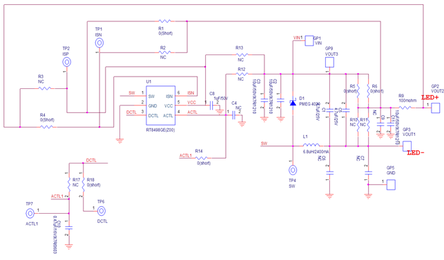
Schematic, Bill of Materials & Board Layout
EVB Schematic Diagram
Bill of Materials
|
Reference
|
Qty
|
Part number
|
Description
|
Package
|
Manufacturer
|
|
U1
|
1
|
RT8498GE
|
|
SOT-23-6
|
Richtek
|
|
C1, C5
|
2
|
GRM31CR71H475KA12L
|
4.7µF/50V/X7R/1206
|
C-1210
|
muRata
|
|
C2, C3
|
2
|
C3216X5R1H106K160AB
|
10µF/50V/X7R/1206
|
C-1210
|
TDK
|
|
C4
|
1
|
|
NC
|
C-0805
|
|
|
C6, C7
|
2
|
|
NC
|
C-1210
|
|
|
C8
|
1
|
C2012X7R1H105KT
|
1µF/50V/X7R/0805
|
C-0805
|
TDK
|
|
C9, C11
|
2
|
|
NC
|
C-1210
|
TDK
|
|
C10
|
1
|
C1608X7R1C474K000N
|
0.47µF/16V/X7R/0603
|
C-0603
|
TDK
|
|
D1
|
1
|
|
PMEG 4020
|
D-CR-73
|
NXP
|
|
L1
|
1
|
NRS8040T6R8NJGJ
|
6.8µH
|
L-SU1028
|
TAIYO YUDEN
|
|
R1, R4
|
2
|
|
Short
|
CP-0603
|
|
|
R2, R3
|
2
|
|
NC
|
CP-0603
|
|
|
R5, R6
|
2
|
|
SHORT
|
CP-0805C
|
|
|
R9
|
1
|
2512T-1-R100
|
100mohm
|
RC-1A
|
RALEC
|
|
R10, R11, R12, R13
|
4
|
|
NC
|
R-0805
|
|
|
R14
|
1
|
RTT05000JTP
|
0R/0805
|
R-0805
|
RALEC
|
|
R17
|
1
|
|
NC
|
R-0603
|
|
|
R18
|
1
|
WR06X000 PTL
|
0R/0603
|
R-0603
|
WALSIN
|
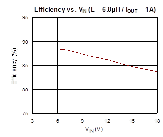
Efficiency:
|
VIN (V)
|
IIN (A)
|
VOUT (V)
|
IOUT (A)
|
Eff. (%)
|
ISP-ISN (mV)
|
|
4.5
|
0.834
|
3.405
|
0.974
|
88.369
|
97.9
|
|
7
|
0.538
|
3.395
|
0.978
|
88.165
|
98.3
|
|
10
|
0.379
|
3.382
|
0.974
|
86.915
|
97.9
|
|
12
|
0.317
|
3.372
|
0.972
|
86.162
|
97.7
|
|
15
|
0.257
|
3.369
|
0.97
|
84.771
|
97.6
|
|
18
|
0.216
|
3.368
|
0.966
|
83.68
|
97.3
|
Line regulation:
|
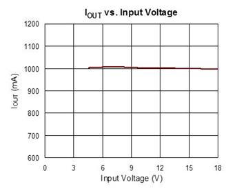
|
|
VIN (V)
|
IOUT (A)
|
|
4.5
|
995.2
|
|
7
|
986.1
|
|
10
|
981.8
|
|
12
|
981.5
|
|
15
|
979.1
|
|
18
|
976.8
|
|
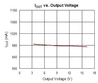
Load regulation:
|
|
|
LEDs
|
VOUT (V)
|
IOUT (mA)
|
|
5LED
|
16.21
|
974.8
|
|
4LED
|
12.88
|
977.5
|
|
3LED
|
9.38
|
978.1
|
|
2LED
|
6.46
|
980.5
|
|
1LED
|
3.38
|
983.8
|
|
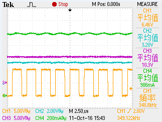
Waveform:
|
Test condition:VIN = 10V, VOUT
= 3V, IOUT = 1A
|
|
CH1 = SW, CH2 = VOUT, CH3 = VIN, CH4 = IL
|
CH1 = SW, CH2 = VOUT, CH3 = VIN, CH4 = IOUT
|

|
|
Analog / PWM Dimming :
PCB Layout
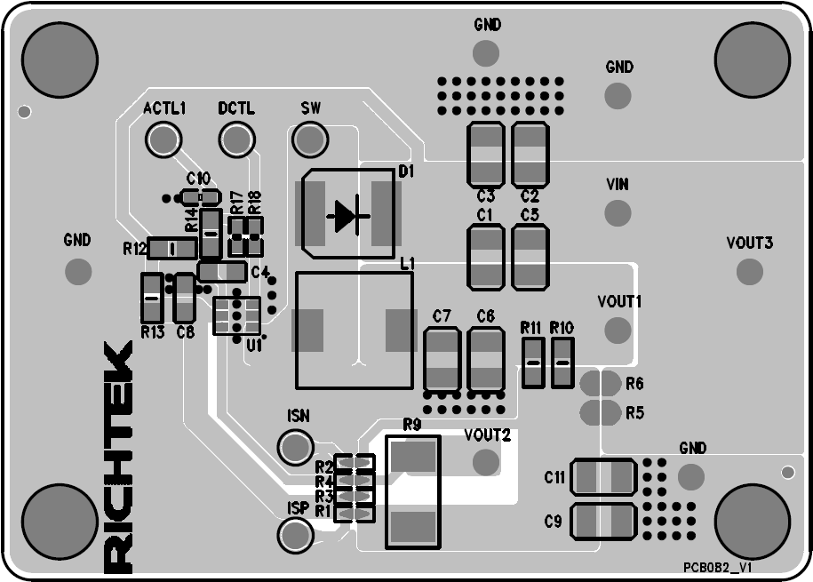
Top View (1st layer)
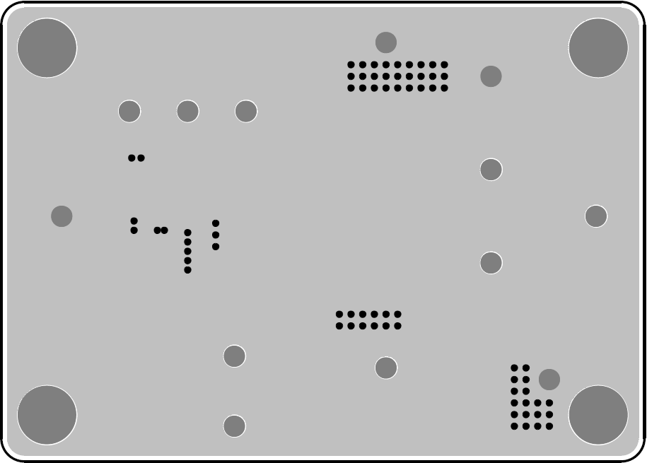
Bottom View (4th Layer)