Analyzing VIN overstress in Power ICs
Abstract
Failures in power ICs are often the result of Electrical Over Stress (EOS) on the IC input supply pin. This report explains the structure of power IC input ESD protection and how ESD cells can become damaged due to EOS. Common causes for input EOS are hot-plug events and other transient effects involving wire or trace inductance in combination with low ESR ceramic capacitors. Solutions are presented how to avoid EOS via special circuit and system design considerations.
1.
Introduction
|
When component failures happen during design or manufacturing process, finding the root cause of the component failure is not always easy, especially if it concerns a sporadic failure that cannot be repeated. ICs that have failed catastrophically will show severe burn marks and analyzing a failed component is sometimes like walking through a burned down house, trying to find the cause of the fire.
At Richtek we have analyzed quite a few failed components from customer application failures. By careful inspection of damage areas, it is sometimes possible to pinpoint the specific failed device, which can help in finding the most likely failure cause.
In many cases, the failure cause is due to too high input voltage.
The following chapters describe a buck converter power IC input structure and the failure mechanism due to input voltage overstress. Several applications are examined on how excessive input voltage can happen and solutions are given how to avoid it.
|
|
2.
Buck Power IC input structure
Figure 1 shows the basic block diagram of a buck converter IC with various ESD protection cells.
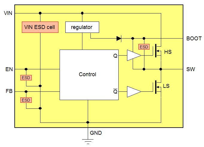
Figure 1
The input supply pin is protected via a large ESD cell, which basically protects the regulator and MOSFETs from high ESD voltage. The SW pin often does not have an ESD cell, because the large MOSFETS themselves can act as ESD clamp, either via their body diodes to ground or VIN ESD cell, or by their own breakdown characteristics. The BOOT pin has an ESD cell to SW pin, and the small signal pins each have a small ESD cell as well, which together with some input series resistance protects the small signal section from high ESD voltages.
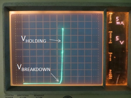
In Richtek power ICs, the ESD device for protecting an IC pin is chosen such that it will become active at a voltage level which is below the device breakdown region, but above the device absolute maximum operation voltage, to avoid unwanted ESD cell activation during operation. See Figure 2.
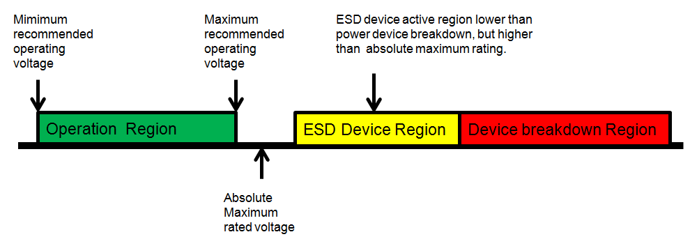
Figure 2
The ESD cell design properties will determine the ESD breakdown voltage, maximum surge capability and snap-back characteristics.
3.
Difference between ESD and EOS
When an overvoltage happens on an IC pin which exceeds the ESD clamp level, the chance of device failure depends on the amount of energy that is dissipated in the ESD device during breakdown.
Both ESD (Electro Static Discharge) and EOS (Electrical Over Stress) are related types of voltage overstress. But there is a clear difference between the two :
- ESD is a very high voltage (> 500V) with relatively short duration (< 1µsec)
- EOS is a moderate voltage (< 100V) with longer time span (normally > 1µsec)
Richtek IC ESD cells are designed to survive the energy of an ESD pulse based on Human Body Model (HBM) 2kV per JESD22-A114 standard and Charged Device Model (CDM) 500V per JESD22-C101E standard. HBM ESD consists of a sharp pulse of roughly 300nsec with exponential decay. CDM ESD consists of a short ring pulse, with ring period of around 4nsec. Of the two types, HBM ESD has the highest energy level. ESD generally is a very short duration event : Figure 3 shows the JEDEC HBM test method, where a 100pF capacitor is charged to a certain level and then discharged via a 1500Ω resistor into the Device Under Test.
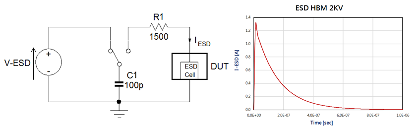
Figure 3
Since most DUT have an ESD breakdown voltage much lower than the test voltage, the ESD peak current is mostly determined by the test voltage and the 1500Ω resistor. In the example waveform a 2kV test voltage results in a 2kV/1.5k = 1.3A peak current. The RC time constant is around 150nsec, so the waveform decays quickly, within 1µsec. For the 2kV ESD test, the charge integral IESD*t is around 0.2µCoulomb. This value can be used to calculate the energy surge in an ESD cell with a certain breakdown voltage during the ESD event. For example, the energy surge during the 2kV HBM pulse in an ESD cell with 27V breakdown voltage is roughly 0.2µC*27V = 5.4µJoule. The energy surge for a 4kV ESD pulse is roughly double this value, around 10.8µJoule.
When a longer time span EOS event happens, the energy surge in the ESD cell during the EOS event is often larger than during an ESD event, and can easily exceed the ESD cell maximum surge energy capabilities. This will cause excessive heating in the silicon around the ESD cell structure, resulting in permanent damage to the ESD cell. Very often, circuitry adjacent to the ESD cell will sustain damaged as well.
4.
Example of IC failure due to Vin overstress
To illustrate an actual IC VIN stress limit, let’s examine RT7285CGE, an 18V rated 1.5A ACOT buck converter in SOT23-6 package. The RT7285C datasheet shows the following Recommended Operating and Absolute Maximum ratings :
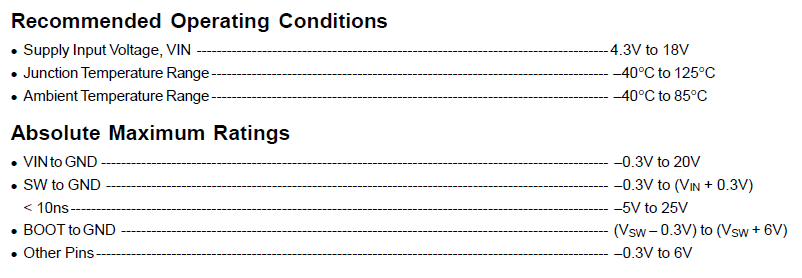
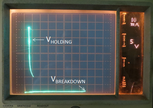
The VIN ESD cell breakdown region will lie above the Absolute Maximum rating of 20V. It is possible to measure the actual ESD breakdown voltage by means of a curve tracer : The curve tracer should be connected between VIN and GND pin. The IC enable pin should be connected to GND to keep the IC in shut-down mode during the measurement. The curve tracer is set for 100µA/div vertical scale, and a low power limit of 0.5W. Then the horizontal voltage is slowly increased. It can be seen that the RT7285C VIN ESD cell breakdown lies around 25.5V, and rises sharply but without snap-back. As long as the current is not too high (< 1mA) and curve tracer power limit is kept low, this measurement will not easily damage the part. See Figure 4.
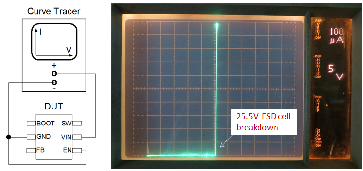
Figure 4
Due to the sharp clamping of the ESD cell breakdown characteristic, any input voltage that exceeds the clamp level will quickly lead to high currents and high dissipation in the ESD cell. Excessive current will quickly lead to damage. If you increase the current and power setting of the curve tracer during VIN ESD cell breakdown measurement, you’ll eventually damage the ESD cell, which can be seen as a sudden collapse of the breakdown characteristic, after which the part will show a low impedance resistive VIN-GND characteristic.
(In continuous mode setting, the curve tracer pulse duration is long, around 4msec, which quickly leads to high energy levels during the higher current testing)
It is possible to do a more precise measurement of the actual ESD cell failure point, by applying a pulsed current to the device under test as shown in Figure 5. The test circuit supply voltage should be above the device breakdown voltage to keep the current source in linear operation. The pulse width and current amplitude can be carefully adjusted to see the ESD cell failure point at various current levels and pulse durations.
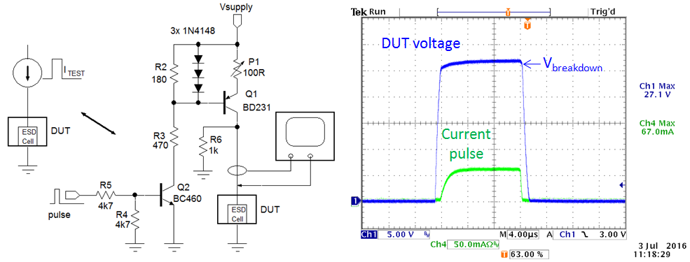
Figure 5
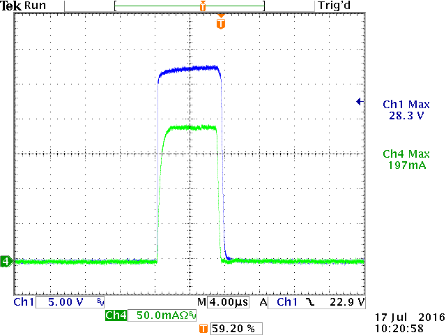
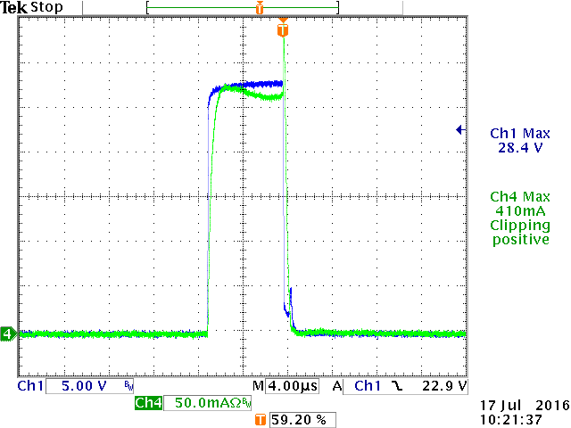
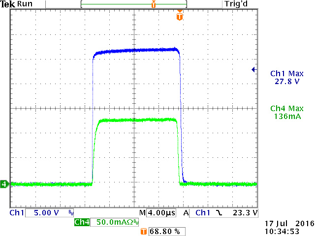
Figure 6 shows the measurements of ESD cell pulse current in breakdown for RT7285C at 25°C using test circuit of Figure 5.
|
Current = 197mA, Δt = 7µsec
No failure
|
Current = 268mA, Δt = 6.2µsec
Failure at the end of the pulse
|
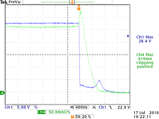
Failure point zoom-in
VESD collapses to ~ 3V
|
|
|
|
|
|
Current = 136mA, Δt = 14µsec
No failure
|
Current = 175mA, Δt = 11.1µsec
Failure at the end of the pulse
|
Failure point zoom-in
VESD collapses to ~ 3V
|
|
|
|
|
Figure 6
From the test waveforms where failure occurs, the ESD cell maximum surge energy can be calculated; it was found that with 6µsec pulse at 268mA (7.6W peak power), the max surge energy is 47µJoule, where as a 11µsec pulse at 175mA peak current (4.9W peak power), the max surge energy for device failure is around 55µJoule. The maximum surge energy where failure occurs is highly dependent on the device temperature : at higher temperature the device will fail earlier than at cold temperatures. But in all cases, the maximum surge energy level in this EOS test is several factors higher than the surge energy during normal HBM ESD events.
Figure 7 shows the de-cap analysis on a parts that failed in the above test. It can be seen that the ESD cell shows burn marks, and the ESD cell ground traces also show slight burn marks at certain spots. Furthermore the high side MOSFET area adjacent to the ESD cell shows some damage as well. This damage indicates severe heating in the ESD cell area.
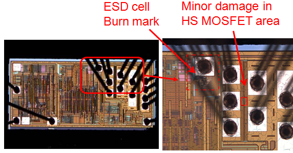
Figure 7
It should be noted that this input voltage overstress was done with the IC in non-operating mode; only the input voltage ESD cell was activated, and maximum current was limited. This gives relatively small silicon die damage.
5.
VIN EOS due to supply hot-plug
One of the common reasons for power IC VIN EOS is power supply hot-plug events. Hot plugging a live power lead into an application that has low ESR ceramic input capacitors can lead to high voltage spikes on the application input due to resonance of the input capacitors with the supply leads. Figure 8 shows a hot-plug example : The power supply is first switched on, and then the leads are connected to the application, where switch S represents the hot-plug action.
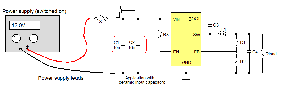
Figure 8
The amplitude of the voltage ringing that will occur on the input capacitors depends on several factors : The internal impedance of the power supply, the lead wire resistance and inductance and coupling, the resistance of switch S and the value and ESR of the application input capacitors C1 and C2.
Let’s for example assume a 12V power supply with big buffer capacitors, two separate low resistance power supply leads with total length of 1.2m, low impedance switch S and two MLCC capacitors of 10µF/25V X5R 1206 size.
The power supply leads total inductance will be around 1.5µH and the resistance including connectors is around 10mΩ. The two capacitors will have a total capacitance of around 9µF at 12V DC due to DC bias effect and have 5mΩ ESR each.
A quick simulation of the hot-plug event with this input circuit is shown in Figure 9.
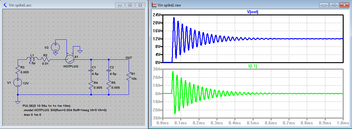
Figure 9
It can be seen that the input current during hot-plug is quite high around 30A and the resonance of the leads inductance and input capacitors can result in a voltage ringing spike of almost double the DC voltage value.
The same hot-plug circuit was tested as shown in Figure 10 : The switch S was replaced by a low Rdson MOSFET switch driven by a pulse generator to make the hot-plug switch action stable and repeatable.
Figure 10
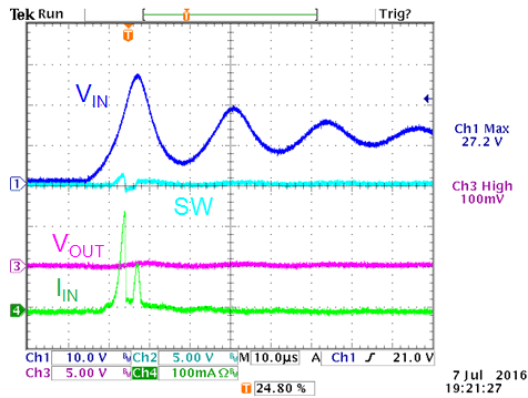
The measurement result is shown in Figure 11 left side :
Figure 11
It can be seen that the actual hot-plug event shows even higher voltage spike than the theory would suggest : This is because of the non-linear capacitance-DC bias behavior of the MLCC input capacitors as shown on the right side. When the voltage across the capacitor rises, the capacitance drops, and the current will charge the smaller capacitor to a higher voltage. In this case, the 12V hot-plug event can result in a maximum voltage spike of around 30V.
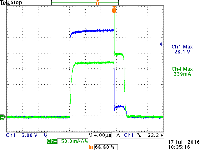
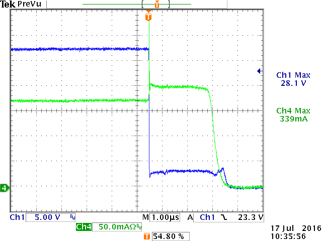
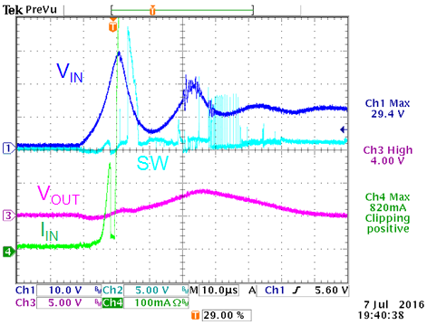
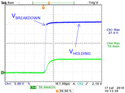
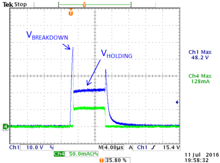
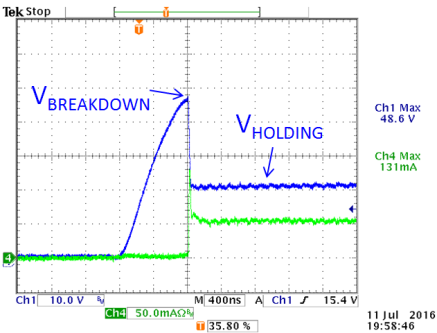
The same hot-plug method was applied to a standard 12V to 5V application of RT7285CGE, and the IC input voltage and IC input current were measured during the hot plug event.
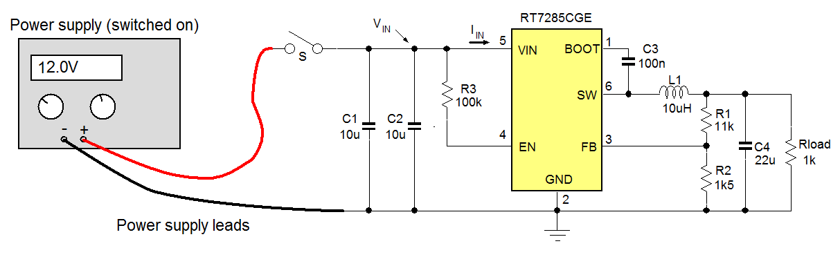
By slowly increasing the supply DC voltage it was possible to observe the IC input current at different VIN peak voltage levels. In operation mode there is an initial IC input current peak which is caused by the bootstrap circuit activation, which should be ignored. The IC input peak current that happens during the supply voltage peak is the ESD cell breakdown current.
|
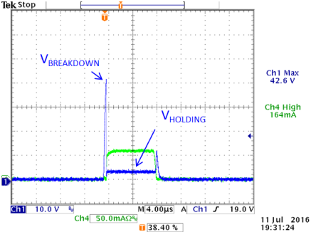
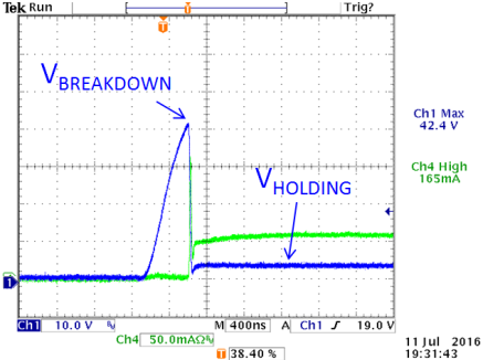
VSUPPLY = 11.6V, VIN peak = 27.2V
|
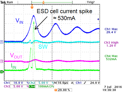
VSUPPLY = 11.9V, VIN peak = 28.4V
|
VSUPPLY = 12.1V, VIN peak = 29.4V
|
|
|
|
|
|
ESD cell breakdown current : 100mA
|
ESD cell breakdown current : 532mA
|
Failure : current runaway, abnormal SW
|
The duration of the current spike is around 1.8µsec. The energy level just before failure was found to be 0.6A*1.8µsec*29V = 31µJoule, more than five times higher than the 2kV HBM ESD pulse energy.
When input voltage overstress occurs during operation mode like the above example, damage to the ESD cell will be bigger due to higher current levels because there is no input current limit, and further damage will occur due to malfunction of the power stage, which normally leads to shoot-through and complete burn-out of the MOSFET section as shown in de de-cap of a Vin overstress failure during operation mode. (Figure 12)
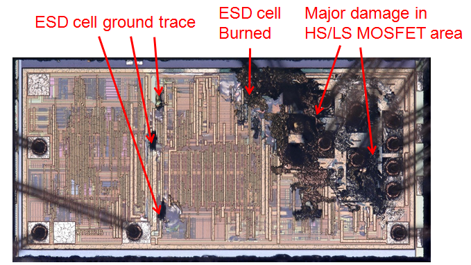
Figure 12
6.
Breakdown characteristics of different ESD cell
types
Depending on IC design and process, different types of ESD cells can be used :
-
PNP type ESD cells will clamp the voltage at a relatively fixed voltage at the breakdown point. They behave more or less like zener diodes. These types are most often used for input protection of DC-DC converters. See Figure 13.
|
25V PNP ESD cell curve tracer plot
|
PNP ESD cell pulse characteristic
|
PNP ESD cell (zoom trigger)
|
|
|
|
|
Figure 13
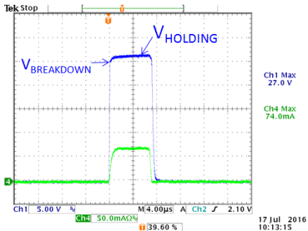
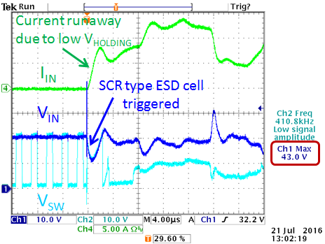
- SCR type ESD cells will latch to a very low voltage when their breakdown voltage is reached, resulting in very hard snap-back action. See Figure 14.
|
40V SCR ESD cell curve tracer plot
|
SCR ESD cell pulse characteristic
|
SCR ESD cell pulse (zoom trigger)
|
|
|
|
|
Figure 14
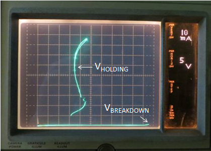
- NPN type ESD cells also show a latch snap-back behavior after breakdown, but their holding voltage is much higher compared to SCR ESD cells. See Figure 15.
|
48V NPN ESD cell curve tracer plot
|
NPN ESD cell pulse characteristic
|
NPN ESD cell pulse (zoom trigger)
|
|
|
|
|
Figure 15
ESD discharge is a short duration current limited event so SCR and NPN ESD cells are very effective in protecting sensitive circuits from high voltages because of their low clamp (holding) voltages. But when these types of ESD cells are triggered during normal operation with DC supply voltage applied, the low holding voltage will cause high input currents when the applied DC voltage is higher than the holding voltage, resulting in immediate destruction. See the below example :
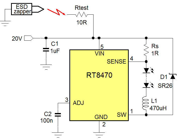
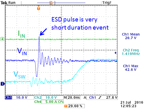
RT8470 is an old generation buck LED driver. The VIN ESD cell is an SCR type. When this ESD cell is triggered due to a short pulse on the VIN pin, the SCR latches and the input supply will be virtually shorted to GND by the ESD cell. This is illustrated in Figure 16 :
|
A short electrical pulse is induced on the VIN supply during operation by means of an ESD gun (or modified gas igniter)
|
The electrical discharge results in a short voltage spike (~5nsec) on VIN. Here the voltage is just not sufficient to trigger the ESD cell.
|
When the SCR ESD cell triggers, it latches to low holding voltage. Supply will be shorted by the ESD cell, leading to high current and IC destruction.
|
|
|
|
|
Figure 16
7.
Solutions to reduce voltage spike during hot-plug
Chapter 5 explained the background of the voltage spike that can occur during power supply hot-plug events. Figure 17 shows the input circuit with all relevant parameters : Supply with low Ri, supply cable with inductance and low resistance and the input capacitor with low ESR. (see Figure 17).
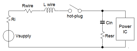
Figure 17
There are several ways to reduce the voltage ringing amplitude during hot-plug :
Solution 1 : The input supply is often a switch-mode adapter with large output capacitors. The output impedance of these circuits is quite low, and hot-plug events can quickly generate high currents. By adding a common mode choke and a small high ESR electrolytic capacitor like shown in Figure 18 right side, the output impedance of the adapter will increase, and the small electrolytic capacitor + ESR COUT1 will help damp resonances.
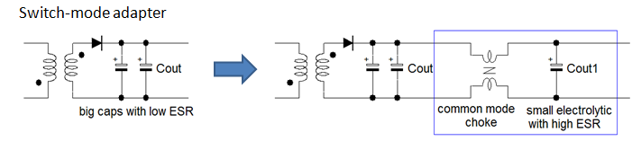
Figure 18
Solution 2 : Increase cable resistance by using adapter cable with smaller wire diameter. For good resonance damping, the cable resistance needs to be larger than 0.3Ω. This will of course increase cable voltage drop.
Solution 3 : Increase the coupling between + and – supply wires : Better coupling between positive and negative wire will cause the opposing magnetic fields of the wires to increase the resonance damping. Figure 19 shows a simulation with 75cm 18AWG coaxial cable, where the wire coupling was estimated to be around 0.8 based on leakage inductance measurements.
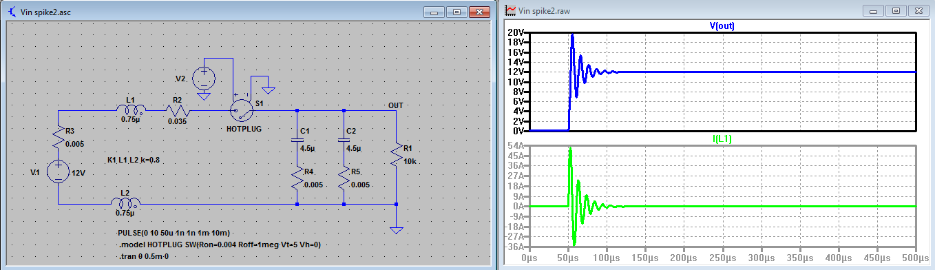
Figure 19
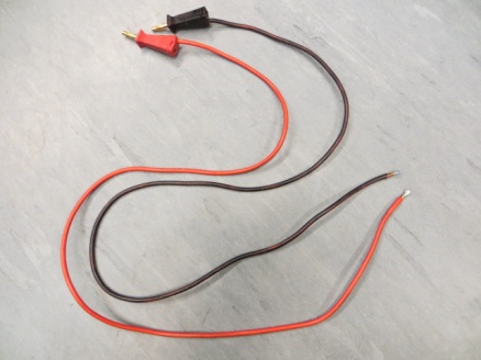
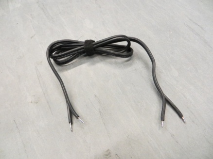
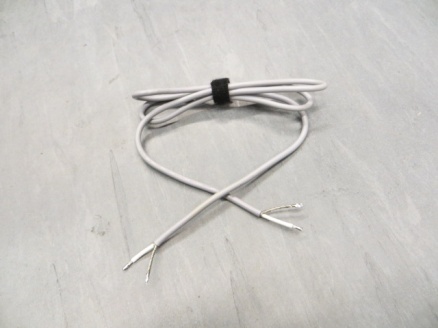
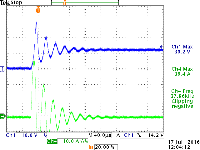
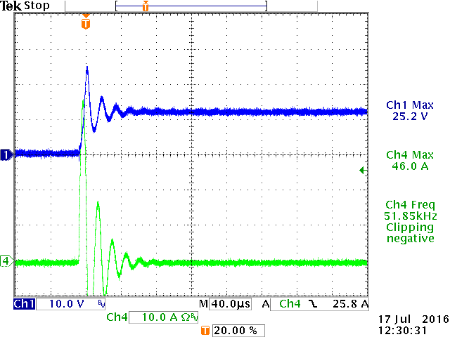
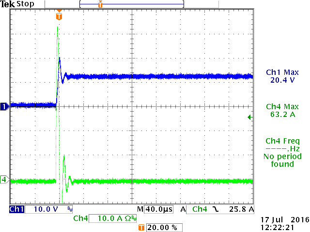
Actual measurement with different wire types confirms that better wire coupling will increase resonance damping and reduces hot-plug voltage spikes. See Figure 20.
|
75cm 12AWG 2.05mm ø lab cable
Coupling < 0.1, Rwire = 0.008Ω
|
75cm 18AWG 1.02mm ø twin cable
Coupling ≈ 0.3, Rwire = 0.035Ω
|
75cm 18AWG 1.02mm ø coaxial cable
Coupling ≈ 0.8, Rwire = 0.035Ω
|
|
|
|
|
|
|
|
|
|
FRESONANCE = 37kHz, VSPIKE = 30.2V
|
FRESONANCE = 51kHz, VSPIKE = 25.2V
|
FRESONANCE = 91kHz, VSPIKE = 20.4V
|
Figure 20
Solution 4 : The resonance ringing of an LC circuit can be damped by placing an RC snubber in parallel with the application input capacitor : The component values for the RC snubber can be calculated as following :
RS can be calculated from  where LP is the cable inductance, CIN is the application input capacitance and ξ is the desired circuit damping.
From the previous hot-plug example, LP was around 1.5µH, CIN was 9µF at 12Vdc. When we choose good damping (ξ = 1), we get RS = 0.2Ω. The value for the snubber capacitor CS needs to be large enough to avoid too high charge during the hot-plug current pulse. VC = IC * 1/ωC where ω is the LP & CIN resonance frequency (measured around 40kHz). The current pulse was 35A, so for less than 2V of voltage increase we need more than 70µF.
We ran the simulation from previous hot-plug example with added 100µF and 0.2Ω RC snubber added :
It can be seen that the resonance is now fully damped and voltage overshoot is less than 2V. See Figure 21.
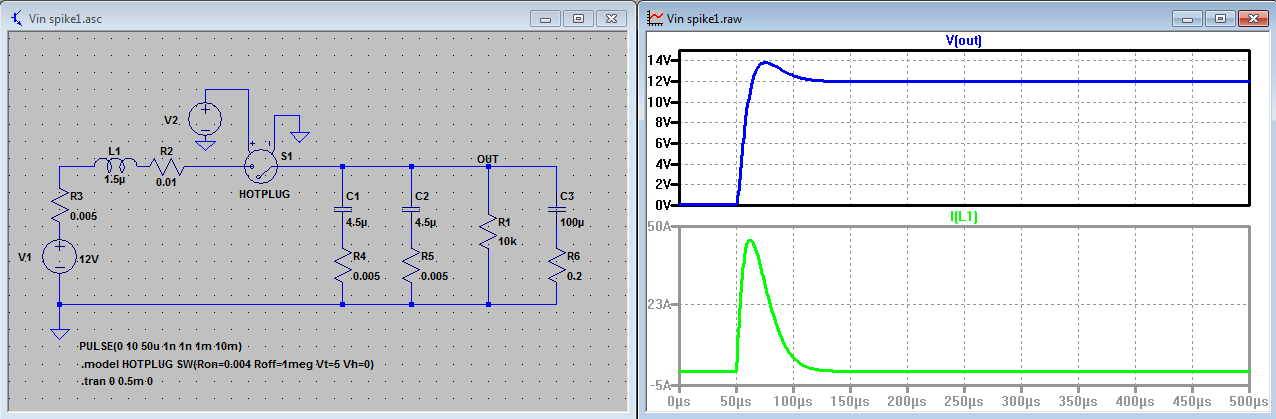
Figure 21
In practical case, the RC snubber can be easily achieved by simply placing a 100µF/25V electrolytic capacitor in parallel with the ceramic input capacitors. (most 100µF electrolytic capacitors have around 0.2Ω ESR at 100kHz).
Figure 22 right side shows the result of the hot-plug event with added 100µF/25V electrolytic capacitor added at the application input. The VIN overshoot is well suppressed and will not give any risk for IC damage.
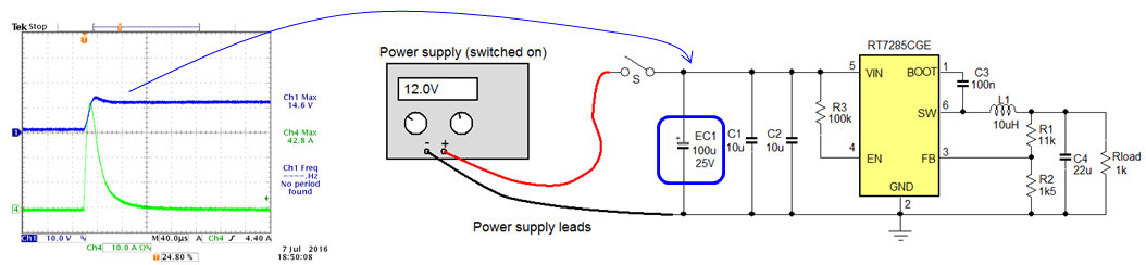
Figure 22
8.
Other causes for power IC VIN EOS
Besides input hot-plug spikes, here are some other practical cases that can result in VIN EOS on power ICs :
a. USB switch input damage during output short-circuit test
Figure 23 shows a typical USB switch application where a small 1µF supply decoupling capacitor is placed close to the IC input. There is a 10cm copper trace from this capacitor to the main 5V system supply.
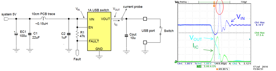
Figure 23
USB ports need to be tested on short-circuit conditions. When the output is shorted with a switch, the IC needs to detect this short-circuit condition and then quickly shut down the pass MOSFET. In the example in Figure 23, the MOSFET shut-down action is has some delay, and momentarily large currents flows through the IC. Then the MOSFET switches off quickly. Due to the input wire inductance, there will be a resonance between this inductance and the small 1µF decoupling capacitor C2. As can be seen on the scope plot, the IC VIN shows a high voltage pulse, which can quickly exceed the IC absolute maximum ratings and result in IC failure.
To solve this potential reliability problem, similar solutions as with supply hot-plug can be considered. In this case, an RC snubber in the form of an electrolytic capacitor at the IC input can be used. Calculation of the snubber is similar, and for the capacitance value calculation the current switch-off dI/dt can be used. A 47µF electrolytic capacitor will reduce the supply voltage spike to around 6V. See Figure 24.
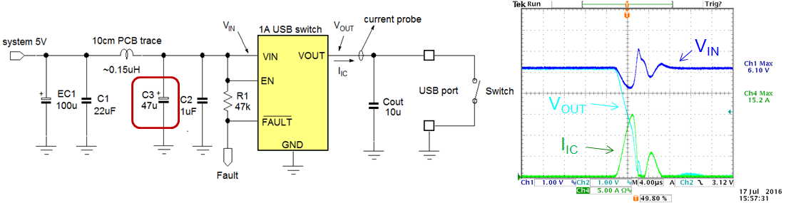
Figure 24
Richtek new generation USB switch family RT9742 has anticipated above short-circuit issue and greatly improved the short circuit detection time, thereby avoiding large currents during short-circuit test. Figure 25 below shows that even with 1µF input capacitor, the IC input voltage stays within safe operation region.
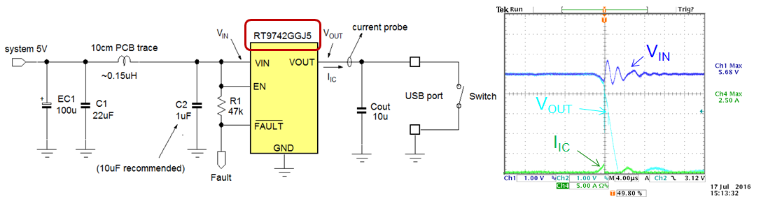
Figure 25
b. Buck converter supply back-biasing
Force-PWM buck converter ICs like RT7285C can act as boost converters when the output is back-biased :
When the output voltage is externally biased above the regulated supply voltage, the IC low side MOSFET will start to sink current from the output, and will form a boost converter with the high side MOSFET. See Figure 26, where a 5V supply is slowly back-biased. Input voltage rises up to the ESD breakdown voltage.
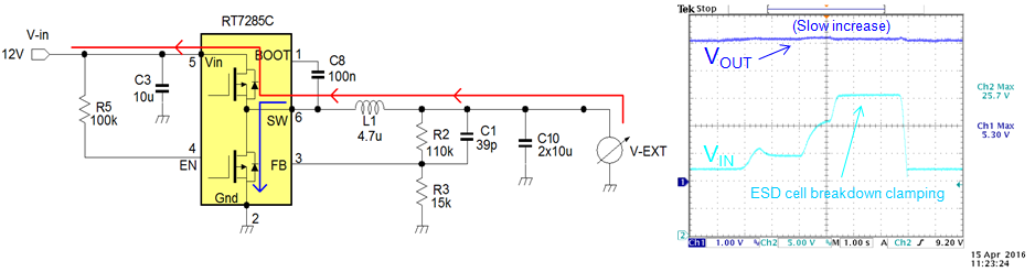
Figure 26
Supply back-biasing does not happen often, but it can occur when there are batteries in the system, or when dynamic supply voltage adjustment is used (dynamic VOUT adjustment via FB network): when the output capacitor is large and VOUT is suddenly reduced, boost action can happen.
When using PSM version ICs (pulse skip mode ICs) the low side MOSFET cannot sink current and with these ICs the back-bias boosting will not happen.
c. Two stage solutions with high impedance feedback network.
Two stage step-down solutions often contain one higher voltage part stepping down to a voltage lower than 5V. A second 5.5V rated converter can be connected to the lower voltage to provide a second low voltage supply rail. In Figure 27 a 17V current mode buck RT8297B steps down the 12V to 3.3V, and an LDO RT9193-25 steps down the 3.3V to a low noise 2.5V.
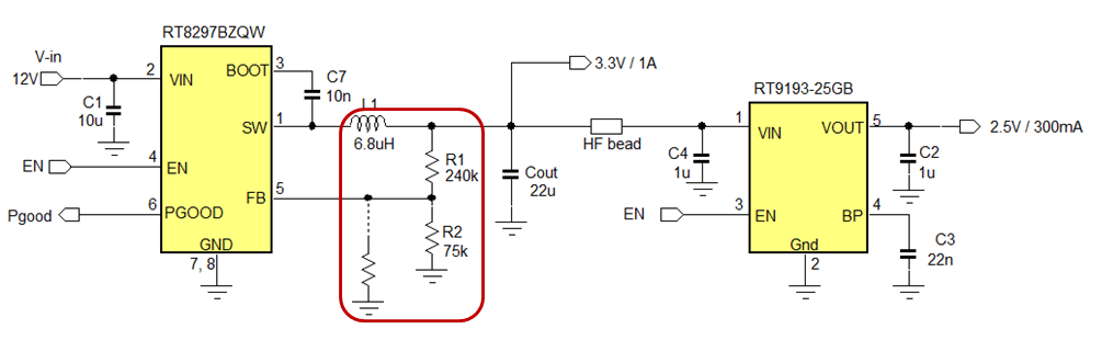
Figure 27
RT8297B is a buck converter with internal compensation. The value of feedback resistor R1 will influence the error amplifier gain and must be selected for suitable crossover frequency. In this example, a single 22µF output capacitor is used, requiring a larger value for R1 to maintain stable operation. The higher R1 value gives a somewhat higher impedance feedback network. This is normally not a problem, unless the feedback network can be touched by a finger, or when there could be PCB leakage to ground, in which case the FB pin of the converter can be disturbed, leading to higher output voltages. Too high output voltage can damage the LDO.
Some circuit designers adopt the finger touching test : They touch different points of the PCB with their fingers and watch for voltage disturbance that can highlight sensitive traces or high impedance. ACOT® converters or current mode converters with GM type error amplifiers have more freedom in feedback network impedance, and could be considered as alternative in this case.
9.
DIY tools for generating EOS
Here are some handy DIY tools for stress testing applications via pulsing currents, electric fields and magnetic fields.
a. ESD zapper (Figure 28)
This is a simple tool made from a modified piezo gas lighter. (The ones without battery or flame).
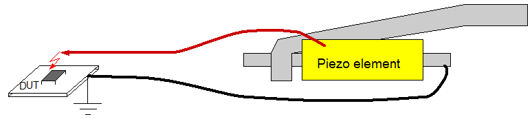
Figure 28
This tool generates high voltage pulses like an ESD gun. Be careful not to shock yourself!
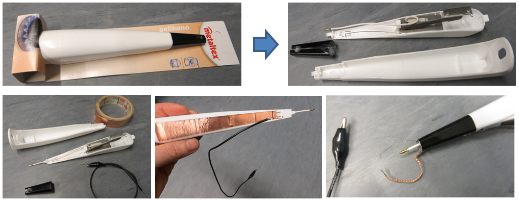
Figure 29
To build this, open up a piezo gas lighter, remove the metal sleeve, pull the high-voltage wire to the outside, use copper tape to cover the hand-grip, connect the piezo ground to the copper and a ground wire. Assemble the metal sleeve again, make sure it connects to the copper tape. You can add an extra ground wire to the sleeve for lower GND impedance to DUT. See Figure 29. Don’t zap ICs directly, but you can zap between different grounds or supply to ground. You can also zap supplies via a series resistor for more quantified behavior.
b. Electric pulsing field generator. (Figure 30)
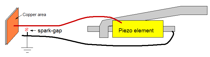
Figure 30
This tool can be derived from the ESD zapper. Connect a copper plane to the high voltage node, and add a spark-gap between high voltage and ground. See Figure 31.
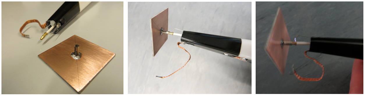
Figure 31
You can use this tool to check your application robustness regarding fast changing electric fields. Mostly high impedance circuits will be affected.
c. Magnetic pulse field generator. (Figure 32)
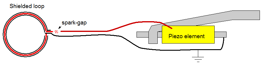
Figure 32
This tool generates a fast changing magnetic field by sending a pulse current through a loop.
You can build this tool using again a piezo gas lighter. You need to make a mounting fixture for an external loop. It is convenient to mount a mini coaxial connector to the front of the piezo lighter. This allows for connection of different loops.
A small double sided PCB can be used as mounting base for the connector, and the PCB can then be soldered to the metal sleeve. You need to add the same copper tape grounding to the gas lighter handle, which must be connected to the piezo ground and metal sleeve. Adjust the high-voltage wire to get around 2~3mm spark-gap. The shielded loop can be build in the same way as the EMI tools loop antenna (see Richtek application note AN045), by soldering the end of the inner wire to the shield of the cable. See Figure 33.
You can use this tool to check your application on sensitive loops. IC supply decoupling loops can be tested in this way. You can also induce pulse currents in cables by coupling the loop via a ferrite core to cables. (similar to EMI common mode current measurements, but now the loop antenna becomes the transmitter). Note that this tool can generate nasty pulses, don’t use it nearby sensitive digital circuits.
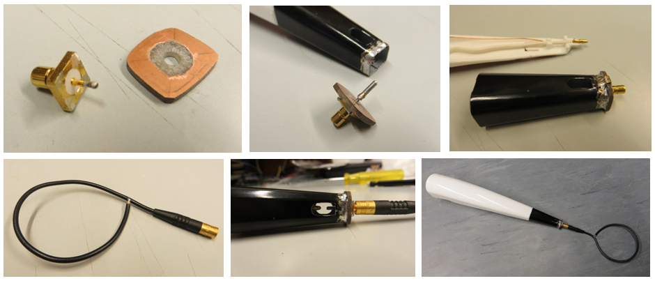
Figure 33
10.
Summary
Power IC damage often occurs due to input voltage overstress. This can happen due to hot-plug voltage spikes or other transients involving wire or copper trace inductance and low ESR ceramic capacitors.
Power IC input pin ESD cells will fail when their maximum surge energy level is exceeded. This EOS energy is normally several factors higher than a normal HBM ESD energy surge. When ESD cells fail, adjacent circuitry in the silicon die will often be damaged as well. In most cases this adjacent circuit damage will lead to power stage malfunction, resulting in shoot-through and power stage burnout. ESD cell types with snap-back may have holding voltage below operating voltage, which can cause high currents as soon as the ESD cell is triggered during operation.
Hot plug events and other resonance effects in power supply wires can cause high voltage spikes on IC inputs. The power design should be checked in these kinds of transients, and counter measures should be taken to avoid high voltage spikes under any operating condition. Although ESD cell breakdown voltage normally lies well above the device absolute maximum ratings, these maximum ratings should not be exceeded in order to guarantee that ESD cells will not become activated during operation.
References :
Fundamentals of Electromagnetic Compatibility 2nd edition, by B. Danker